


Research Article
Determining Optical Constants of Sol-Gel Vanadium Pentoxide Thin Films using Transmittance and Reflectance Spectra
1Department of Physics, Yarmouk University, Jordan
2Department of Physics, Jordan University, Jordan
*Corresponding author: Nehad M Tashtoush, Professor, Department of Physics, Yarmouk University, Jordan, E-mail: nehadmt@yu.edu.jo
Received: June 21, 2019 Accepted: June 29, 2019 Published: July 9, 2019
Citation: Tashtoush NM, Sheiab A, Jafar M, Momani S. Determining Optical Constants of Sol-Gel Vanadium Pentoxide Thin Films using Transmittance and Reflectance Spectra. Int J Phys Stud Res. 2019; 2(1): 59-64. doi: 10.18689/ijpsr-1000108
Copyright: © 2019 The Author(s). This work is licensed under a Creative Commons Attribution 4.0 International License, which permits unrestricted use, distribution, and reproduction in any medium, provided the original work is properly cited.
Abstract
Vanadium pentoxide (V2O5) thin films have been prepared by Sol-Gel technique. The fluid resin which was prepared by dissolving V2O5 powder (99.6%) in H2O2 was spin coated on a glass substrate at room temperature. The effect of preparation conditions, such as spin speed and acceleration, on the film thickness has been investigated. Speed was found to be the most affecting parameter on the film thickness. Transmittance and reflectance spectra were made at normal incidence on these films in the range of 350-900 nm. SCOUT program was used to find out the thickness of all samples. In the region of the fundamental absorption edge, the absorption coefficient was calculated directly from the experimental transmittance and reflectance data using a formula that is nearly valid for non-uniform in homogeneous films. Moreover, the band-gap energy was found to be around 2.3 eV. The refractive index of the films was calculated using PUMA code which is based on a certain fitting procedure for transmittance spectra according to Swanepoel formula. All results were in good agreement with those found in literature.
Keywords: Vanadium pentoxide; Sol-Gel; Optical Constants; Spin coating; Refractive index; Absorption coefficient; Extinction coefficient; Swanepoel formula.
Introduction
Because of its useful electrical, catalytic and electrochemical properties, V2O5 thin films have been widely studied during the past few decades. Heating in vacuum or reducing atmosphere due to partial dissociation are reasons that make V2O5 loses oxygen. This results in the formation of defects or reduced phases [1]. Moreover, V2O5 thin films were applied in the construction of various electro- optical devices such as: thermoelectric sensors, light modulators, and electro-chromic electrodes [2]. The performance of devices utilizing V2O5 films depends on their film quality, which is determined by the morphology, crystalline, degree of disorder, stoichiometry that are highly dependent on the film-deposition method and preparation conditions such as the environmental atmosphere, deposition temperature, deposition rate, and post-deposition heat treatment [3-5]. Therefore, many techniques have been used to prepare V2O5 thin films [3-15]. In this study, sol-gel technique with spin coating method will be used to prepare V2O5 thin films to investigate their optical properties.
The optical constants of a material describe how the characteristics of light are affected when it interacts with the material. The most important optical constants are the ordinary index of refraction (n), the absorption coefficient (α) and the extinction coefficient (k). These optical constants are important factors in understanding the quality and performance of films incorporating in the design of electronic devices used in the various applications. In principle, the optical constants of solid-state layers can be determined by transmittance T and/or reflectance R measurements. For a linear, homogenous, uniform thin film of thickness d and complex refractive index (N=n−ik) with smooth plane-parallel surfaces laid on a polished thick substrate of refractive index ns, the analysis yields Swanepoel T-formula for ideal {air-thin film-dielectric thick substrate-air}-structure, which is given by [16,17]:
In which the absorption parameter x is related to absorption coefficient α of the film as

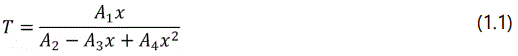
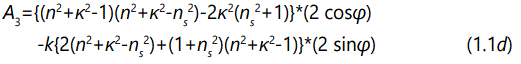
And the parameter A1, A2, A3, and A4 are described by the following expression


where φ is the optical path difference arising from a double traversal of the light plane wave inside the film, and is given by

Experimental Details
In order to prepare high quality V2O5 films, it is necessary to use clean and good quality substrates to insure a good adhesion between film and substrate. The glass substrates, used for this study, were dipped in a saturated potassium dichromate solution in concentrated sulfuric acid for 24 hours. This solution helps in removing grease, pigments and other contaminants from substrates surfaces that might affect adhesion and structure of the obtained films. Then, the substrates were rinsed by distilled water in ultrasonic bath for 10 minutes. After this, the slides were washed by soap water before dipping in acetone, and then cleaned by methanol. Finally, the slides were heated up at 100°C for about 5 minutes before placed in a desiccator to avoid their pollution with dust and other air contaminants.
V2O5 sol-gel was prepared by dissolving 2 grams of the 99.6% purity V2O5 powder (Aldrich) in 120 ml of 15% H2O2 solution under vigorous agitation for 6 hours [15]. Then, the obtained red brownish solution was transformed into a viscous solution after direct heat treatment at 70°C for 20 mins with non-stop agitation. Many films were prepared under different deposition conditions at room temperature using spin coating method. A small puddle of a fluid resin was either deposited onto the center of a substrate and then spinning the substrate at high speed to thin the fluid (the static dispense), or dispensing while the substrate is turning at low speed about 500 rpm (the dynamic dispense). This spin-coating process was achieved by the use of a commercial NXG spinner. The operation of this spinner can be programmed through one step or several steps with the speed ranges from 100 rpm to 10000 rpm with many options for acceleration.
X-ray Shimadzu XRD-6000 X-Ray Device with a copper target has been used to measure XRD pattern for all samples. In order to measure the transmittance and reflectance spectra, a NanoCalc-XR spectrophotometer (Metrology systems and Ocean Optics, Germany) was used to measure the transmittance and reflectance spectra of the samples. This spectrophotometer has the advantage of having an optical wavelength resolution of 0.1 nm and the spot size of the coming light beam can be varied in the range of 200 μm, which will assist in minimizing the effect of the non-uniformity of the film.
Results and Discussion
In this study, the transmittance T (λ) and reflectance R (λ) spectra will be used to investigate most of the optical properties of the prepared sol-gel thin films in addition to determining its thickness. In order to achieve this, two analytical approaches will be used. The first is using SCOUT software which will be mainly used to measure the thickness of the film by fitting the transmittance and/or reflectance spectrum. SCOUT is a type of a numerical curve-fitting procedure, which will be employed for analyzing the results of transmittance and reflectance of films taken by use of the NanoCalc-XR system. Such SCOUT software contains a variety of dispersion dielectric functions that one either can revert to them when necessary or can build up his own dispersion relation. The second approach that will be used has been developed by Chambouleyron and his colleagues, and referred to as PUMA code [18]. In brief, PUMA is unconstrained optimization program that implements an unconstrained formulation of a nonlinear programming model, which solves the problem using a method based on repeated calls to an unconstrained minimization algorithm, without implying a specific functional relationship for the dispersion of the optical constants of the film under investigation. PUMA will be used to analyze the theoretical normal-incidence Swanepoel T-formula, i.e. Eqn. (1.1). The refractive index of the samples will be determined using this analytical Code.
Effect of preparation conditions on film thickness
The spin coating process involves several major factors that generally define the final film thickness, such as the acceleration, spin time, and spin speed which is the most important factor in this process, where it affects the degree of radial (centrifugal) force applied to the liquid resin. A number of samples were prepared to investigate this effect on the thickness of the deposited films. The dependence of thickness on the spin speed is shown in figure 1.
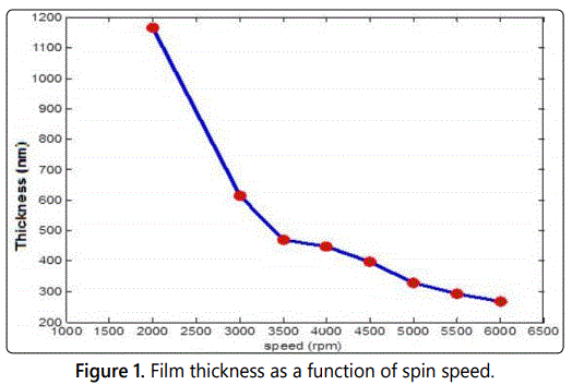
As illustrated in figure 1, a decrease in the film thickness is observed as spin speed increases. Films with high speed possess low values of thickness. Sample of 2000 rpm speed has a thickness value of 1164 nm while that of 6600 rpm speed possess a value of 268 nm. This result is reasonable and acceptable since the more speed means more centrifugal force and then more particles (mass) just move away of the center which leads to less thickness. Figure 2 shows the behavior of the thickness as a function of acceleration. As shown, it seems that the acceleration affects the film thickness but not as much as the speed.
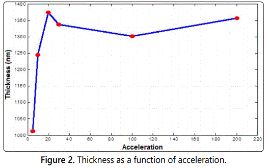
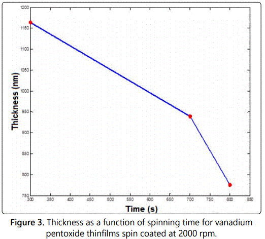
As indicated in figure 2, the film thickness increases dramatically for low values of acceleration. However, for large values of acceleration the thickness seems to be constant. This sounds to be normal behavior since all the material on the disk will spread out all over the substrate in the first few seconds of starting acceleration. Increasing acceleration then will not affect the little residual amount of mass over the disk. Finally, figure 3 shows the behavior of film thickness as a function of spinning time. As shown in the figure, the film thickness decreases as the time increased. This is due to the fact that the more spinning time with a certain angular velocity the more expansion of the material of the film over the substrate. Also, when the film was exposed to more spinning time, more evaporation occurs which means less thickness.
XRD measurements
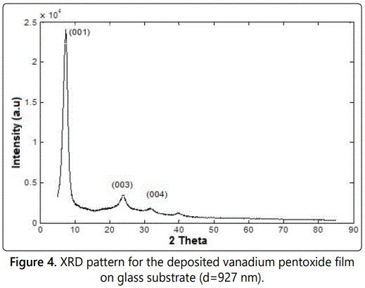
A typical XRD pattern of the deposited sample of thickness 927 nm is shown in figure 4. Three peaks were revealed from this sample. The peaks are located at about 8°, 24° and 32°, corresponding to (001), (003) and (004) crystal planes of V2O5 xerogel, which is the characteristic of the layered structure of the V2O5 xerogel film [19]. All other samples show the same behavior.
Transmittance and reflectance spectra
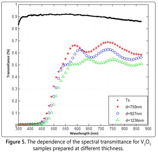
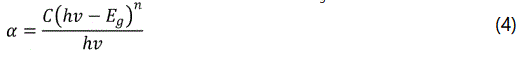
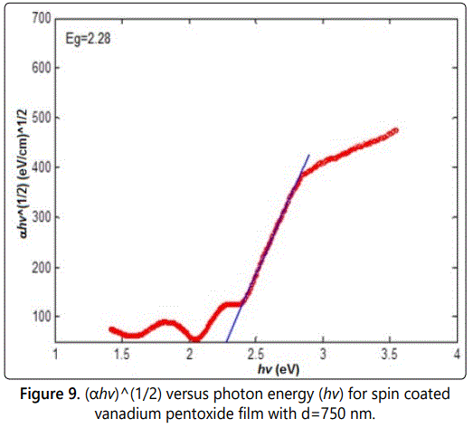
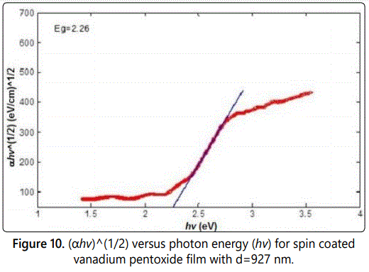
In order to investigate the optical properties, three samples were prepared. The samples were identified by the symbols s1, s2, and s3 with thicknesses of d1=750 nm, d2=927nm, and d3=1236 nm, respectively, as determined by using SCOUT-program analysis. Both transmittance T(λ) and reflectance R(λ) spectra have been measured at normal incidence as a function of the spectral wavelength λ in the range of 350-900 nm. Figure 5 shows the transmittance behavior as a function of wavelength for the three samples. It is clear that the T-spectrum curves for all samples display a few broad and ill-resolved interference-fringes, indicating that a shrinkage phenomenon of interference maxima and mina was taking place probably due to non-uniformity of the films and/or clustering, roughness and no homogeneity of such films. Also, the figure shows the measured T-λ spectrum of a typical bare glass substrate which is used to check out the effect of the deposited film on the transmittance spectrum.
It is noticed that the measured film transmittance decreases as its thickness increases. The behavior of transmittance spectra in the supposed transparent region cannot be explained mainly due to optical absorption in the film, but more likely due to shrinkage of the T-maxima due to non-uniformity, roughness, etc. of these films, which should approach that of bare substrate in such an optically transparent region [16]. Further, one can notice that the optical absorption of the films is fairly strong near the absorption edge of vanadium pentoxide located around the spectral wavelength λ=540 nm, but the decline in this absorption region is not steep, suggesting that the produced films were not well crystalline.
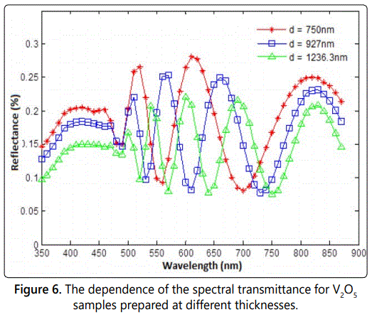
The measured reflectance R(λ)-λ curves of the three samples are presented in the figure 6. Figure 6 indicates that the behavior of the reflectance is as expected for semiconducting oxides in the sense it displays well-resolved interference-fringe maxima and minima, the positions of which are opposite to those observed for the respective transmittance spectra, indicating a total π-phase difference occurring upon reflection from the structure. The number of interference-fringe extremes is different from sample to sample, depending on the thickness of the material. Furthermore, the height of the maxima in the measured R(λ)-λ curves decreases monotonically with decreasing wavelength, while it decreases with increasing the thickness of the sample.
Determining absorption coefficient
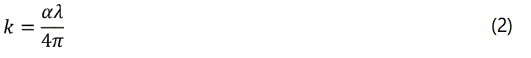
The absorption coefficient α is of a great importance in optical applications. It is related to the extinction coefficient k(λ) by the relation
The absorption coefficient (α) is related to the measured transmittance and reflectance by the relation:
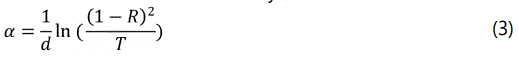
This will be used in calculating the absorption coefficient of the samples [20].
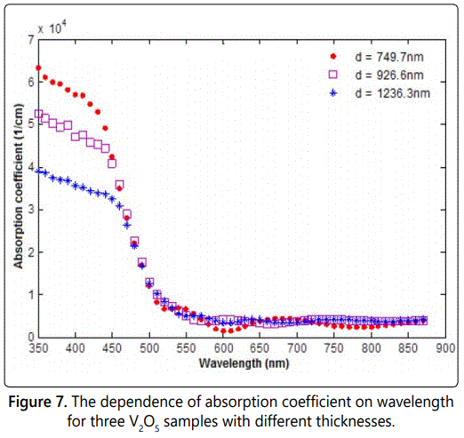
As indicated in figure 7, the absorption coefficient of s1 is d=750 nm) that decreases from more than 6.35 × 104 cm-1 to less than 1.2 × 104 cm-1 in the range of 350 to about 500 nm. After this value of wavelength, the absorption coefficient has an average value of about 0.5 cm-1. This shows that the film has a high absorption at values of wavelength less than about 500 nm, but higher transmission at the higher region of the spectrum. The other two samples show similar behavior to the first sample of absorption coefficient as function of wavelength for the others samples. It is very clear that the absorption coefficient of wavelength less than 500 nm, is strongly dependent on the film thickness, since we can notice that the absorption coefficient as function of wavelength of the thickness 926 nm, the absorption coefficient values change from (5.1 × 10⁴ –1.005 × 104 cm-1), while the values change from (3.8 × 10⁴ –0.7285 × 104 cm-1) for the sample of thickness 1236 nm.
Calculation of extinction coefficient
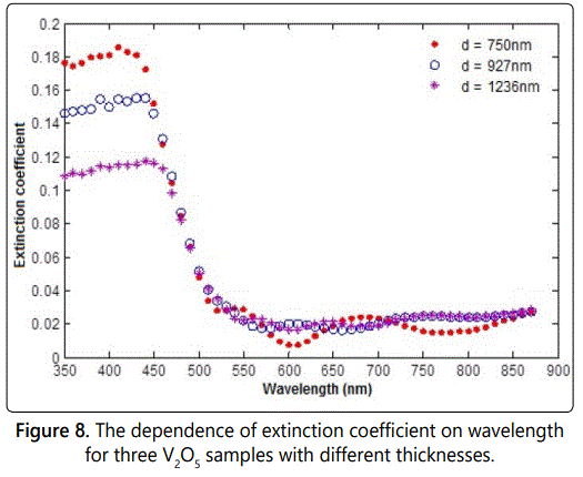
The extinction coefficient is a measure of energy loss and directly related to the absorption coefficient according to the relation (4.1). The calculated values of absorption coefficient in the previous section were used to calculate the extinction coefficient κ for all samples of our study. The dependence of extinction coefficient on the wavelength is shown on figure 8 for the samples.
Itʼs clear that, as the figure 8 shows, the extinction coefficient has a sharp decrease in the range (450-500 nm) for almost all the samples. Then, the extinction coefficient of the samples changed up and down in the wavelength range of (500-900 nm).
Determination of the energy gap
The fundamental absorption edge of semiconductors corresponds to the threshold for charge transitions between the highest nearly filled band and the lowest nearly empty band for a photon has energy much less than the energy gap the absorption is very small and increases significantly for higher photon energies.
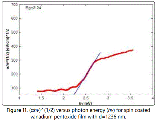
The forms of the absorption coefficient as a function of photon energy depend on the type of energy bands containing the initial and final states. The absorption coefficient is described in terms of the photon energy hv and the direct allowed band gap energy Eg by the relation [11,20].
where C is the probability parameter for the transition, h is the Plankʼs constant, and v is the photon frequency. The exponent n takes the values 1/2 or 3/2, depending on whether the transition is an allowed or forbidden direct band-to-band transition, respectively. The optical energy gap of each film was estimated from the optical measurements. The absorption coefficient for indirect allowed band gab was found to be following the relation (4) with n equal to 2.
Figures 9–11 show the relation between αhv1/2 as a function of the photon energy in the absorption region for the three samples s1, s2, and s3 respectively. The energy band gap can be determined from the extrapolation of the linear portion with the photon energy axis. The value of the energy band gap was decreased as the thickness increased. Moreover, the values obtained are in consistent with other values obtained by literature [15].
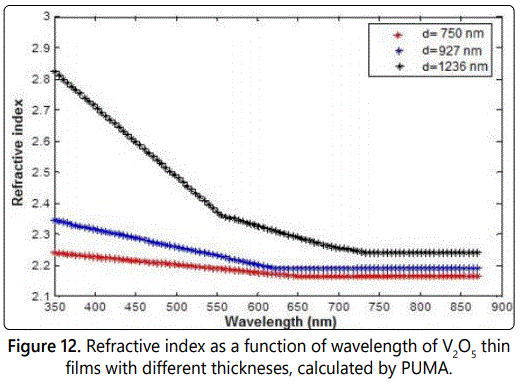
Determining refractive index
Refractive index can be calculated in many different ways, one of which is using PUMA program. The refractive index n(λ) results obtained by PUMA computational program are illustrated in figure 12.
As indicated in figure 12, the refractive index decreases as wavelength increases. It is clear that the refractive index n increases as the film thickness increases. The refractive index is related to the density and the polarizability of a certain material [21]. Thus changing the film thickness could change the density of V2O5 thin film. The maximum value of refractive index is about 2.8 for the thicker film (d=1236 nm) in the value of 350 nm. This behaviour is in good agreement with what is known about the behaviour and values of refractive index as a function of wavelength.
Conclusions
V2O5 thin films have been prepared using sol-gel spin coating method. The effect of preparation conditions were investigated. It was found that the spinner speed is the main factor that affects the thickness. The film thicknesses and then the optical constants were determined and investigated using a specific program named SCOUT. The films showed a small transmittance rage in the VIS region, from 550 nm to 850 nm, with max transmittance of about 70%. The absorption coefficient was calculated for each sample and shows a normal behaviour and magnitudes that reflects the behaviour of the obtained transmittance and reflectance spectra. The band gap energy, calculated from the absorption relation with photon energy, was found to be about 2.3 eV which is inconsistent with other values found in literature. Finally, the refractive index was calculated using a certain program code called PUMA which depends on analyzing and fitting the experimental transmittance data. These results using this approach of analysis will help in going forth in more studies and analysis of V2O5 to explore its importance in photocell industry especially after dopping with some proper nanomaterials and in chemical gas sensing as it shows very large response to a certain gases in nature.
Acknowledgment
The authors would like to thank Yarmouk University represented by the deanship of graduate studies and scientific research for funding this research through the grant No. 29/2011. The grant assists in finishing up two master theses, one of which this article is summarized, and was done by the student Afaf Sheiab.
References
- Ramana CV, Mahammad Hussain OM. Optical absorption behaviour of vanadium pentoxide thin films. Advanced Materials for Optics and Electronics. 1998; 7: 225-231. doi: 10.1002/(SICI)1099-0712(199709)7:5<225::AID-AMO309>3.0.CO;2-R
- Golan G, Axelevitch A, Sigalov B, Gorenstein B. Investigation of phase transition mechanism in vanadium oxide thin films. Journal of Optoelectronics and Advanced Materials. 2004; 6: 189-195
- Julien C, Guesdon JP, Gorenstein A, Khelfa A, Ivanov I. The growth of V2O5 flash-evaporated films. J Mater Sci Lett. 1995; 14(13): 934-936.
- Wu X, Lai F, Lin L, et al. Influence of thermal cycling on structural, optical and electrical properties of vanadium oxide thin films. Appl Surf Sci. 2008; 255(5): 2840-2844. doi: 10.1016/j.apsusc.2008.08.048
- Baddour-Hadjean R, Golabkan V, Pereira-Ramos JP, Mantoux A, Lincot D. A Raman study of the lithium insertion process in vanadium pentoxide thin films deposited by atomic layer deposition. J Raman Spectrosc. 2002; 33(8): 631-638. doi: 10.1002/jrs.893
- Su Q, Pan X, Xie E, Wang Y, Qiu J, Liu X. Influence of temperature on the microstructure of V2O5 film prepared by DC magnetron sputtering. Rare Metals. 2006; 25(6): 82-87. doi: 10.1016/S1001-0521(07)60050-3
- Meng LJ, Silva RA, Cui HN, Teixeira V, dos Santos MP, Xu Z. Optical and structural properties of vanadium pentoxide films prepared by d.c. reactive magnetron sputtering. Thin Solid Films. 2006; 515(1): 195-200. doi: 10.1016/j.tsf.2005.12.061
- Okuhara T, Inumaru K, Misono M, Matsubayashi N. Highly Active V2O5 Thin Films Prepared by Chemical Vapor Deposition on Silica for Oxidative Dehydrogenation of Alcohols. Stud Surf Sci Catal. 1993; 75: 1767- 1770.
- Ramana CV, Hussain OM, Uthanna S, Srinivasulu Naidu B. Influence of oxygen partial pressure on the optical properties of electron beam evaporated vanadium pentoxide thin films. Opt Mater (Amst). 1998; 10(2): 101-107.
- Akl AA. Thermal annealing effect on the crystallization and optical dispersion of sprayed V2O5 thin films. J Phys Chem Solids. 2010; 71(3): 223-229. doi: 10.1016/j.jpcs.2009.11.009
- Tashtoush NM, Kasasbeh O. Optical Properties of Vanadium Pentoxide Thin Films Prepared by Thermal Evaporation Method. Jordan Journal of Physics. 2013; 6(1): 7-15.
- Iida Y, Kanno Y. Doping effect of M (M = Nb, Ce, Nd, Dy, Sm, Ag, and/or Na) on the growth of pulsed-laser deposited V2O5 thin films. J Mater Process Technol. 2009; 209(5): 2421-2427. doi: 10.1016/j.jmatprotec.2008.05.033
- Bouzidi A, Benramdane N, Nakrela A, et al. First synthesis of vanadium oxide thin films by spray pyrolysis technique. Mater Sci Eng B Solid State Mater Adv Technol. 2002; 95(2): 141-147. doi: 10.1016/S0921-5107(02)00224-6
- Julien C, Khelfa A, Guesdon JP, Tuncheva V, Gendron F. Electrical properties of flash-evaporated V2O5 films. Ionics (Kiel). 1996; 2: 380-385.
- Benmoussa M, Outzourhit A, Jourdani R, Bennouna A, Ameziane EL. Structural, optical and electrochromic properties of sol-gel V2O5 thin films. Active and Passive Electronic Components. 2003; 26(4): 245-256.
- Swanepoel R. Determination of the thickness and optical constants of amorphous silicon. J Phys E. 1983; 16(12): 1214-1222. doi: 10.1088/0022-3735/16/12/023
- Abdul-Gader Jafar MM. Comprehensive formulations forthe total normalincidence optical reflectance and transmittance of thin films laid on thick substrates. European International Journal of Science and Technology. 2013; 2(5): 214-274
- Chambouleyron I, Martinez JM. Optical properties of Dielectric and Semi conductor thin films. In: Nalwa HS (ed). Handbook of Thin Films. Chapter 12, Volume 3. New York: Academic press. 2001.
- Jin A, Chen W, Zhu Q, Yang Y, Volkov VL, Zakharova GS. Structural and electrochromic properties of molybdenum doped vanadium pentoxide thin films by sol–gel and hydrothermal synthesis. Thin Soild Films. 2009; 517(6): 2023-2028. doi: 10.1016/j.tsf.2008.10.001
- Al-Assiri MS, El-Desoky MM, Alyamani A, Al-Hajry A, Al-Mogeeth A, Bahgat AA. Spectroscopic study of nanocrystalline V2O5 ·nH2O films doped with Li ions. Optics & Laser Technology. 2010; 42: 994-1003. doi: 10.1016/j.optlastec.2010.01.020
- Minkov DA. Method for determining the optical constants of a thin film on a transparent substrate. J Phys D Appl Phys. 1989; 22(1): 199-205. doi: 10.1088/0022-3727/22/1/029
