

Research Article
A Reliable Device Topology for ZnO Nanowire-based Gas Sensors
1Department of Electrical Engineering, City University of New York, USA
2Intel Corporation, Portland Oregon, USA
*Corresponding author: Bruce C Kim, Professor, Department of Electrical Engineering, City University of New York, USA E-mail: bkim@ccny.cuny.edu
Received: April 3, 2019 Accepted: May 3, 2019 Published: May 15, 2019
Citation: Kim BC, Gupta A. A Reliable Device Topology for ZnO Nanowire-based Gas Sensors. Madridge J Nanotechnol Nanosci. 2019; 4(1): 148-153. doi: 10.18689/mjnn-1000129
Copyright: © 2019 The Author(s). This work is licensed under a Creative Commons Attribution 4.0 International License, which permits unrestricted use, distribution, and reproduction in any medium, provided the original work is properly cited.
Abstract
The frontiers of research are rapidly advancing in the area of nanowire-based sensors, which are being used for a breadth of applications. ZnO nanowires-based sensors have shown tremendous potential in the area of chemical and biological sensing but the performance of these sensors are contingent upon the successful design and packaging of sensing platform. Therefore, in this work two distinct device topologies, single ZnO nanowire device and ZnO nanowire-based array device, have been fabricated and compared for their sensing performance. The single nanowire device has been fabricated through focused ion beam and e-beam lithography techniques while SEM and EDAX analysis have been used to characterize the device. I-V characteristics of the ZnO nanowire-based array devices have been measured through a semiconductor parameter analyzer and a prospective device refresh strategy through thermal cycling has been outlined.
Keywords: ZnO nanowires; Single nanowire device; Multi-nanowire device; Gas sensor.
Introduction
Nanostructured materials have been extensively researched for a broad spectrum of applications. Especially, development and application of nanomaterials for chemical and biological sensing have been widely reported [1-7]. In recent literature, a complete review has been done in wireless chemical sensors and biosensors [2]. The unique surface-related properties, with tunable size- and shape-dependent physical and chemical properties, offer great potential for manipulating and improving sensing behavior. These characteristics have been demonstrated to aid in improving sensitivity and response rate of sensors [8,9]. Maturity of synthesis techniques and availability of variety in terms of morphology and structure of these nanomaterials have provided immense flexibility to researchers for application-specific sensor development. These nanosensors have, therefore, proven to be quite useful in areas, such as environmental sensing, homeland security, vehicular emission control, industrial gas detectors, and biosensing.
Specifically, metal oxide nanowire systems are an important class of nanomaterials for sensing a wide spectrum of chemical and biological analytes [10,11]. They are regarded as an important class of materials for sensor development due to the flexibility they offer in terms of carrier modulation and control. Specifically, the electrical characteristics of transition metal oxides can be manipulated through doping or external functionalization that ultimately aids in improving sensitivity and detection limits in differential resistive sensors. The surface structure of these nanostructured oxides is also conducive to adsorption/desorption-based modes of sensing. For example, Zhang et al. demonstrated the use of single indium oxide (In2O3) nanowire to detect nitrogen dioxide (NO2) and ammonia (NH3) under room temperature conditions [12]. Lowest detectable concentrations of up to 0.5 ppm for NO2 and 0.02% for NH3 were reported. They purported a sensing mechanism dependent on doping of the single In2O3 nanowire. They suggested that upon exposure to NO2 or NH3 the oxygen vacancy concentration on the nanowire surface was modified due to doping from these electron-deficient and electron-rich groups respectively. This resulted in modulation of conductance in the nanowire device due to exchange of electrons between the fermi levels of analytes and the nanowire. Based on a similar concept, Zhou et al. demonstrated a NO2 gas sensor with multiple and single In2O3 nanowire transistor devices [13]. Detection limits of up to 60 ppb range were reported under room temperature conditions.
Among the numerous metal oxide nanomaterial systems, ZnO nanowires have been utilized continuously in different morphologies and topologies to fabricate sensitive detection systems for simple analytes, such as carbon monoxide (CO), NH3, NO2, and humidity (H2O). It is, therefore, befitting at this juncture to highlight some pertinent empirical reports in this area. Wang et al. utilized single ZnO nanowire sensors, fabricated with MEMS technology, for detecting ppm levels of ethanol vapors at 300°C [14]. Similarly, Fan et al. developed a ZnO nanowire field-effect sensor to detect NO2 and NH3 [15]. They observed that the gate potential was related to the device sensitivity and that desorption of analyte molecules from nanowire surface was facilitated by applying a large negative gate bias. This provides an additional pathway for refreshing ZnO nanowire-based sensors. In contrast, Yang et al. used UV properties of ZnO nanowires for developing chemical gas sensors [16].
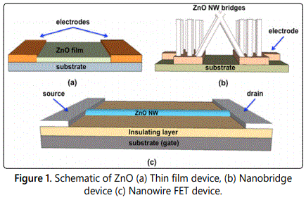
As highlighted above, detailed investigations have been made to study nanomaterials and specifically metal oxide systems, including ZnO, to elaborate their potential as reliable sensing elements for various chemo- and bio-sensor systems [17,18]. However, mere development of sensing chemistry and illustrating sensing behavior under laboratory conditions do not guarantee reliable and sensitive sensor operation in a realistic unpredictable environment [19]. To overcome this challenge and develop high reliability, sensitive, robust, and selective detection platforms requires ingenious design efforts focusing at successful integration of the sensing chemistry with the required hardware. It can be seen that although considerable research is directed towards developing sensing chemistry, focus on sensor design from a device standpoint is more often neglected and conventional approaches are followed. Three major device topologies that are used to demonstrate nanosensor operation are as follows and ZnO nanostructure-based sensors have been selected to explicate the case [20,21]. First, a quite prevalent sensing element configuration involves a film-based design, where a ZnO thin film is grown or deposited between electrodes on a substrate and used as a sensing element, as shown in figure 1a. The advantage of this topology is the simple geometry and cost-effective processing techniques as compared to other complex methods, which makes them lucrative for scaling. However, this topology often compromises on the limit of detection attainable due to limited surface sites available for analyte interaction on ZnO nanofilm. Second morphology comprises ZnO nanostructures as bridges and grown on a substrate to produce a conductive channel for carrier transport. The advantage of this method stems from the greater surface area available for analyte permeation and interaction, which leads to enhanced sensitivity and resolution. The schematic of ZnO nanobridge topology is depicted in figure 1b. Finally, single ZnO nanowire devices either in FET mode or amperometric mode have also been shown to exhibit good sensitivity and resolution under laboratory conditions. A typical configuration of a single ZnO nanowire sensor is shown in figure 1c. The disadvantage of using this approach is the low reliability and robustness of the sensor devices, which leads to incoherent operation under field conditions.
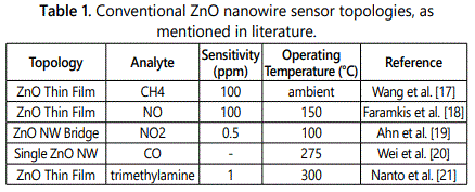
As summarized in table 1, ZnO nanostructures have been widely used in the aforementioned topologies for detecting simple analytes and possess varied limits of detection. However, their field applicability is limited partly due to cost factors and remainder due to the sensing chemistry utilized. Most ZnO nanostructure-based sensors employ amperometric transduction mechanism where a differential change in conductance, produced as a result of analyte interaction with the ZnO nanostructure substrata, is used to establish sensor operation. This mode of sensing severely limits the range of analytes that can be detected and also the sensitivity under ambient operating conditions. On a fundamental level, this change in conductance stems from modulation of oxygen vacancy concentration on nanowire surface upon analyte interaction. The analyte molecules occupy available vacant sites and alter the intrinsic carrier concentration of the nanowires either through electron donation or electron acceptance from the analyte. While this mode of sensing is capable of providing high resolution, its limitations are two-fold. First, sensors relying purely on amperometric mode lack selectivity. Any contaminant with a donor or acceptor site can produce the same change in conductance, which can make de-convolution of actual signal from the total sensor response quite challenging. Second, the sensor operation is severely constrained to simple analyte molecules that can modify surface vacancy concentration through chemisorption only at high temperatures. High temperature reduces the activation energy barrier for chemisorption and lead to enhanced sensitivity. However, high temperature operation is an undesirable characteristic for a field deployable sensor. Hence, through aforementioned discussion it is evident that to develop a nanosensor that is capable of high sensitivity and selectivity towards complex molecules, such as explosives or nitroaromatics, under ambient conditions is a highly desirable objective. It can also be concurred that device topology in concomitance with the appropriate surface engineering of the nanowire substrata would aid in accomplishing the outlined objective.
Therefore, in this work we compare two distinct device fabrication techniques and present a comparative case study for ZnO nanowire sensors for sensitive determination of trace amounts of p-nitrophenol vapor under ambient conditions. First, a single ZnO nanowire device was fabricated by using focused ion beam and E-beam lithography techniques. After appropriate characterization and analysis the drawbacks and limitations of this approach are highlighted. Second, a multinanowire array-based device topology is investigated. Subsequently, its successful operation is demonstrated by using saturated p-nitrophenol as a model analyte under a concurrent opto-electronic excitation. Both devices utilize receptor-functionalized ZnO nanowires. Here in, we would use the sensor chemistry we developed earlier and focus exclusively on device topology and configuration effects on sensor reliability, sensitivity, and selectivity. A refresh strategy for the sensor is also posited.
Experimental Methods
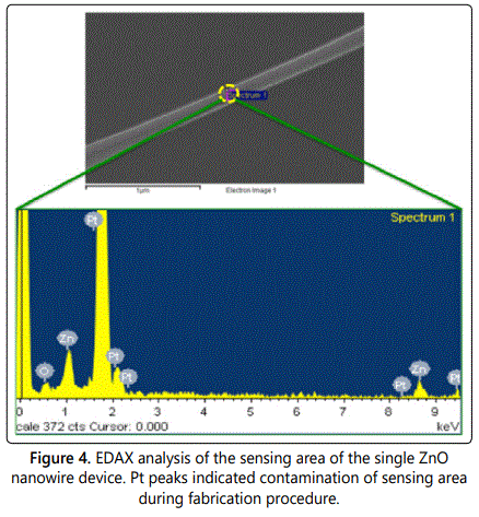
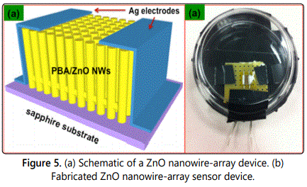
The ZnO nanowires for device fabrication were synthesized through a chemical vapor deposition process as explicated in our previous works. Briefly, ZnO nanowire growth resulted from the templated substrate (sapphire) due to vapor-liquid-solid (VLS) mechanism of nanowire growth at a temperature of 950°C. A single nanowire device was fabricated through extraction and manipulation of a nanowire from the ensemble of nanowires. This was accomplished by using micro-fabrication techniques of E-beam lithography and focused ion beam (FIB). First, inter-digitated electrodes on insulating sapphire substrates were made using E-beam lithography. The substrates were coated with 100 nm of positive resist (PMMA A2) at 4500 rpm for 45 seconds and were baked at 180°C for 90 seconds to make them adequate for the E-beam process. An inter-digitated pattern designed using CAD package with NPGS (Nanometer Pattern Generation System) was written on the resist-coated substrates. The exposed substrates were developed using 1:1 (v/v) solution of MIBK and acetone for 90 seconds. Subsequently, a 70 nm coating of gold was deposited followed by lift-off to complete fabrication of inter-digitated electrode. Thereafter, these substrates were introduced in a focused ion beam (FIB) system (FEI Quanta 3D Dual-beam) along with receptor-functionalized ZnO nanowires on sapphire substrates. A single ZnO nanowire was extracted from the ensemble of nanowires using an in-situ micromanipulator and laid across the inter-digitated electrode. Subsequently, the nanowire was welded at its extremities, where it overlaps the electrode, with platinum using the in-situ GIS (gas injection system) to complete fabrication of the device. Before extracting the single ZnO nanowire device from the FIB chamber, EDAX analysis of the exposed nanowire area was performed. This was done to identify any prospective contamination that might have happened as a result of subjecting the single nanowire to an intense device fabrication procedure. The multi-nanowire device fabrication utilized receptor-functionalized ZnO nanowire arrays on sapphire substrates. To fabricate these devices colloidal silver solution (Ted Pella, Inc.) in a volatile solvent was coated at the extremities of the receptor-functionalized nanowire substrates to function as electrodes. Silver was used to make an ohmic contact between functionalized ZnO nanowires and the electrode.
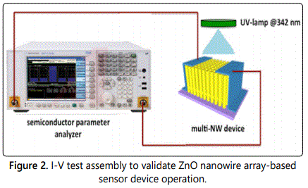
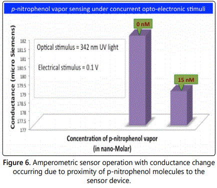
The electrical properties of the multi-nanowire devices were measured using a semiconductor parameter analyzer (Agilent Technologies). I-V curves of both pristine and receptor-functionalized ZnO nanowire array devices were measured. It is to be noted that device testing of single ZnO nanowires was not pursued due to alteration of chemical composition of the device due to unavoidable contamination resulting from the device fabrication procedure. This will be discussed in the forthcoming section. Subsequent to preliminary testing of the functionalized multi-nanowire device, an additional optical stimulus from a 342 nm UV lamp was provided to test for opto-electronic sensing behaviour of the device. Current was then measured from the device under a bias of 0.1V. Subsequently, the device chamber was allowed to saturate from p-nitrophenol vapors by introducing a few milligrams of the solid powder. Current was then measured from this device after 5 minutes to validate the sensing behavior of the device. The test assembly to establish sensor operation is illustrated in figure 2. The benefit of this assembly is that it permits transduction of optical response from the sensor to an amperometric signal, which makes it easier to measure with conventional electronics without the use of sophisticated optical detectors. However, utilizing sophisticated optical detection and transduction electronics will only serve to improve the sensitivity and selectivity of the device in addition to minimal false positive rate.
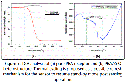
To determine the appropriate refreshing methodology for the fabricated sensor, thermogravimetric analysis (TGA) was used. Nitrogen was used as a purge gas. First, pure receptor powder was tested for weight loss from the range of 25-600°C with the temperature rate of 5°C/min in a TGA/DSC 1-Thermogravimetric Analyzer (Mettler Toledo, Inc.) Values from the blank run were automatically subtracted from the data. Second, receptor-functionalized ZnO nanowire samples were subjected to the TGA analysis under similar experimental conditions. Results from both sets of experiments were used to suggest a possible strategy to refresh the multi-nanowire sensor.
Results and Discussion
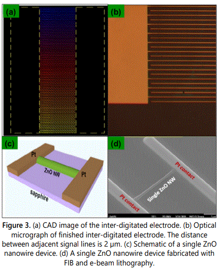
For fabricating a single nanowire device a receptor-functionalized ZnO nanowire was extracted from the ensemble of nanowires grown on the substrate using the micromanipulator in-situ the FIB system and was placed across the inter-digitated electrode. Figures 3a and 3b shows the E-beam mask design and the optical micrograph of the completed electrode, respectively. After successfully positioning the nanowire across the electrodes, platinum was deposited at its extremities to complete the fabrication of the device. Figure 3c exhibits the schematic of the single nanowire device while figure 3d shows the completed device. Before retrieving the finished nanowire device from the FIB system, EDAX analysis of the exposed nanowire area was performed. This was done to ensure the compositional integrity of the sensor device fabrication procedures. It was observed that the platinum deposited was not confined to the electrode area but also contaminated the sensing area resulting in unintentional doping. Figure 4 shows the EDAX spectrum of the selected area on the exposed functionalized nanowire surface. Platinum peaks can be clearly observed, which indicate its incorporation in the sensing area. Pertaining to such findings, the single functionalized ZnO nanowire device was evaluated to be unsuitable for p-nitrophenol sensor fabrication. Furthermore, electrical tests on these single ZnO nanowire devices yielded inconsistent, erratic results confirming unreliability and minimal signal-to-noise.
To investigate the reliability of this device further, the sensing chip was subjected to thermogravimetric analysis (TGA) to determine the breakdown temperature of the PBA/ZnO heterostructure. The opto-electronic sensor operation of the multi-nanowire array device is contingent upon chemical integrity of the heterostructure. Therefore, the advantages of using TGA are two-fold. First, it aids in determination of the temperature range, where the PBA receptor coating would be stable on ZnO nanowire surface. This would serve as a measure to qualitatively determine the robustness of the device under field conditions, since the sensor could be subjected to a varied temperature regime while being deployed on the field. Second, it would allow for identification of a prospective strategy to reset the device. Figure 7a shows the TGA spectrum of pure PBA receptor. It can be observed that in the temperature range of 250-450°C the sample exhibited maximum weight loss, which indicated the decomposition of PBA receptor. This means that the sensor operation limit is less than 250°C. Figure 7b shows a TGA spectrum of PBA-functionalized ZnO nanowire sensors. The maximum weight loss in the sensing chip happened in the range of 250-450°C indicating breakdown of the chemisorped organic layer of PBA on ZnO nanowire surface. This complies with the data for pure PBA decomposition in figure 7a. The data was normalized to minimize the effect of instrument drift. It was especially useful for the analysis of PBA/ZnO heterostructure, where subtle weight changes in the sub-milligram range could be observed. However, drift at large temperatures became large and could not be removed even with normalization.
Based on aforementioned results it was concurred that for developing a reliable ZnO nanosensor device for detecting hazardous compounds, a multi-nanowire array device is a much better alternative than a single nanowire sensor device. While a multi-nanowire device would be easy to interface with back-end electronics, it also exhibits far more reliability in terms of field deployment as compared to a single nanowire device.
Conclusion
Two distinct device fabrication approaches were investigated to determine the most reliable topology of a field deployable ZnO nanosensor device for detecting p-nitrophenol vapors. First, a single ZnO nanowire device was fabricated with E-beam lithography and focused ion beam techniques. The EDAX analysis confirmed unintentional doping of Platinum in the sensing area during electrode deposition, which indicated contamination. Second, a multi-nanowire array approach for device fabrication was investigated. The sensor device exhibited good sensitivity and reliable operation. The temperature resilience of the device was tested through thermogravimetric analysis, where it was determined that the device can be operated up to 250°C. It also suggests that thermal shock to the device can serve as a possible strategy to refresh the device and resume stand-by operation mode. These sensor topologies could be used to develop chemical vapor sensors for detecting explosive materials, carbon monoxide and methane gas.
Acknowledgements
This work was partially funded by the U.S. Army Contract No. W31P4Q-09-D-0028, AMRDEC in Huntsville, AL.
References
- Maduraiveeran G, Sasidharan M, Ganesan V. Electrochemical sensor and biosensor platforms based on advanced nanomaterials for biological and biomedical applications. Biosens Bioelectron. 2018; 103: 113-129. doi: 10.1016/j.bios.2017.12.031
- Kassal P, Stienberg MD, Stienberg IM. Wireless chemical sensors and biosensors: A review. Sens Actuators B Chem. 2018; 266: 228-245. doi: 10.1016/j.snb.2018.03.074
- Polley N, Basak S, Hass R, Pacholski C. Fiber optic plasmonic sensors: Providing sensitive biosensor platforms with minimal lab equipment. Biosens Bioelectron. 2019; 132: 368-374. doi: 10.1016/j.bios.2019.03.020
- Asefa T, Duncan CT, Sharma KK. Recent advances in nanostructured chemosensors and biosensors. Analyst. 2009; 134(10): 1980-1990. doi: 10.1039/b911965p
- Börner S, Orghici R, Waldvogel SR, Willer U, Schade W. Evanescent field sensors and the implementation of waveguiding nanostructures. Appl. Opt. 2009; 48(4): B183-B189. doi: 10.1364/AO.48.00B183
- Murray CB, Norris DJ, Bawendi MG. Synthesis and characterization of nearly monodisperse CdE (E = sulfur, selenium, tellurium) semiconductor nanocrystallites. J Am Chem Soc. 1993; 115(19): 8706-8715. doi: 10.1021/ja00072a025
- Daniel MC, Astruc D. Gold nanoparticles: assembly, supramolecular chemistry, quantum-size-related properties, and applications toward biology, catalysis, and nanotechnology. Chem Rev. 2004; 104(1): 293-346. doi: 10.1021/cr030698+
- Cui Y, Wei Q, Hongkun P, Lieber CM. Nanowire nanosensors for highly sensitive and selective detection of biological and chemical species. Science. 2001; 293(5533): 1289-1292. doi: 10.1126/science.1062711
- Kakati N, Jee SH, Kim SH, Lee HK, Yoon YS. Sensitivity enhancement of ZnO nanorod gas sensors with surface modification by an InSb thin films. Jpn J Appl Phys. 2009; 48(10): 105002. doi: 10.1143/JJAP.48.105002
- Cobden DH. Molecular Electronics-Nanowires begin to shine. Nature. 2001; 409(6816): 32-33. doi: 10.1038/35051205
- Cui Y, Lieber CM. Functional Nanoscale Electronic Devices Assembled Using Silicon Nanowire Building Blocks. Science. 2001; 291(5505): 851-853. doi: 10.1126/science.291.5505.851
- Zhang DH, Li C, Li XL, et al. In2O3 nanowires as chemical sensors. Appl Phys Lett. 2003; 82(10): 1613-1615. doi: 10.1063/1.1559438
- Zhou CW, Zhang DH, Liu ZQ, et al. Detection of NO2 down to ppb levels using individual and multiple In2O3 nanowire devices. Nano Lett. 2004; 4(10): 1919-1924. doi: 10.1021/nl0489283
- Wang TH, Wan Q, Li QH, et al. Fabrication and ethanol sensing characteristics of ZnO nanowire gas sensors. Appl Phys Lett. 2004; 84(18): 3654-3656. doi: 10.1063/1.1738932
- Fan ZY, Lu JG. Gate refreshable nanowire chemical sensors. Appl Phys Lett. 2005; 86(12): 123510. doi: 10.1063/1.1883715
- Kind H, Yan H, Messer B, Law M, Yang P. Nanowire ultraviolet photodetectors and optical switches. Adv Mater. 2002; 14(2): 158-160. doi: 10.1002/1521-4095
- Wang XD, Ding Y, Li Z, Song JH, Wang ZL. Single-Crystal Mesoporous ZnO Thin Films Composed of Nanowalls. J Phys Chem C. 2009; 113(5): 1791-1794. doi: 10.1021/jp809358m
- Farmakis FV, Speliotis Th, Alexandrou KP, et al. Field-effect transistors with thin ZnO as active layer for gas sensor applications. Microelectron Eng. 2008; 85(5-6): 1035-1038. doi: 10.1016/j.mee.2008.01.040
- Ahn MW, Park KS, Heo JH, Kim DW, Choi KJ, Park JG. On-Chip Fabrication of ZnO-Nanowire Gas Sensor with High Gas Sensitivity. Sens Actuators B Chem. 2009; 138: 168-173. doi: 10.1016/j.snb.2009.02.008
- Wei TY, Yeh PH, Lu SY, Wang ZL. Gigantic enhancement in sensitivity using Schottky contacted nanowire Nanosensor. J Am Chem Soc. 2009; 131(48): 17690-17695. doi: 10.1021/ja907585c
- Nanto H, Sokooshi H, Kawai T, Usuda T. Zinc-oxide thin-film trimethylamine sensor with high sensitivity and excellent selectivity. J Mater Sci Lett. 1992; 11(4): 235-237.
