

Research Article
Photo sensivity Hetero junction C-Si/Porous-Si/Zncds
Baku State University, Baku, Azerbaijan
*Corresponding author: Maarif A Jafarov, Baku State University, Baku, Azerbaijan, E-mail: maarif.jafarov@mail.ru
Received: December 26, 2018 Accepted: January 22, 2019 Published: January 28, 2019
Citation: Jafarov MA, Mamedov HM, Nasirov EF. Photo sensivity Hetero junction C-Si/Porous-Si/Zncds. Madridge J Nanotechnol Nanosci. 2019; 4(1): 123-126. doi: 10.18689/mjnn-1000125
Copyright: © 2019 The Author(s). This work is licensed under a Creative Commons Attribution 4.0 International License, which permits unrestricted use, distribution, and reproduction in any medium, provided the original work is properly cited.
Abstract
Nanostructure ZnCdS thin film was fabricated by electro deposition technique. To manufacture the porous-Si, p-type c-Si wafers of (100) orientation were used as a substrate. The anodization of c-Si substrate surface was carried out in Teflon chamber with Pt cathode. HF: ethanol solution were used for the porous silicon formation. The internal structure of the obtained samples was investigated via X-ray diffraction (XRD), atomic force microscopy (AFM), scanning electron microscopy (SEM). The currentvoltage characteristics of the ZnCdS/PS solar cell at dark conditions and under illumination were investigated. The capacitance for Nano-ZnCdS/PS Solar Cell decreases with the increase of the reverse bias voltage and with the increasing of etching time of nPS layers. That hetero junctions demonstrate good photo-response in the wavelength range of 510 ÷ 650 nm.
Keywords: Porous-Si, Electrodeposition, Heterojunctions, Photo-response
Introduction
The II–VI semiconductor nanocrystals exhibit interesting properties and their emission spectra is very narrow (spectrally pure) and the emission colour is simply tuned by changing their size. As the nanocrystal size decreases, the energy of the first excited state decreases qualitatively following a particle-in-a-box behaviour. This size dependence and the emergence of a discrete electronic structure from a continuum of levels in the valence and conduction bands of the bulk semiconductor result from quantum confinement; hence, semiconductor nanocrystals are referred to as quantum dots [1-4].
Cadmium sulfide (CdS), a typical one of II-VI semiconductor materials, has received considerable interest for its useful applications in solar cells, photoconductors, sensors, optical detectors, field effect transistors, light emitting diodes and nonlinear integrated optical devices [5-9]. Owing to its transparency and photoconductivity, CdS thin films are also used widely as n-type window layers for hetero junction solar cells [10-12].
Porous silicon has attracted great attention due to its room temperature photoluminescence in the visible light range. As we know that, the bulk crystalline silicon has an indirect gap at 1.1 eV at room temperature, which results in a very inefficient radiative recombination and produced light in the infrared region. Therefore, the strong visible light emission in porous silicon is quite surprising and such structure can exhibit a large variety of morphologies and particles sizes. Porous silicon shows different features in comparison to the bulk silicon such as shifting of fundamental absorption edge into the short wavelength and photoluminescence in the visible region of the spectrum. However, different hypothesis is reported on photoluminescence from porous silicon surface. Porous silicon consists of a network of nanoscale sized silicon wires and voids which formed when crystalline silicon wafers are etched electrochemically in hydrofluoric acid based electrolyte solution under constant anodization conditions. The precise control of porosity and thickness allows the tailoring of optical properties of porous silicon and has opened the door to a multitude of applications in optoelectronics technology. Such structures consist of silicon particles in several nanometer size separated by voids. Hence, porous silicon layers are regarded as nanomaterials, which can be obtained by the electrochemical etching of silicon water. Porous silicon structures has good mechanical robustness, chemical stability and compatibility with existing silicon technology therefore has a wide area of potential applications such as waveguides, In section two, the synthesis and characterization of electrochemically anodized nanocrystalline porous silicon layers is done, then, the setup was used in fabrication as a device of Nano-CdS/PS hetero junction solar cell, and investigating the electrical properties of the hetero junction [13-14] .
Experiment
To manufacture the hetero junctions, p-type c-Si wafers (2.5 Ohm· cm resistivity and 0.2 ÷ 0.3 mm thickness) of (100) orientation were used as a substrate. Before anodization, the surface of the c-Si substrates were etched in an aqueous solution of HF and further washed in distilled water (at temperature of 80°C) and ethyl alcohol and then dried in air. The anodization of c-Si substrate surface was carried out in Teflon chamber with Pt cathode. HF: ethanol solution (1:1) were used for the porous silicon formation. The anodization voltage, current density and anodization time were 30V, 40-70 mA/cm2 and 30-1800 sec, correspondingly. Depending on the anodization current and time porous-Si with porous size of 7-50 nm were prepared on the surface of c-Si.
After the PS layer formation, samples was immersed into ethyl alcohol, dried in air and placed into the electrochemical bath for the deposition of nanostructure ZnCdS films. Electro deposition of the ZnCdS films onto the c-Si/porous-Si (with porous size of 7.4; 10 and 30 nm) substrates was carried out at temperature of 80°C from aqueous solution containing cadmium (CdCl2), zinc (ZnCl2) and sodium (Na2S2O3) salts. Cyclic voltammetry was used to monitor the electrochemical reactions in solutions of CdCl2 and Na2S2O3, then in their combined solution of the same concentration and pH. The cyclic voltammograms was scanned in the potential range 1.2 V to –1.2 V versus graphite (or Ag/AgCl) electrodes. Depending on the deposition time, substrate pores size and the individual system, ZnCdS films (with thickness up to 0.2 ÷ 0.6µm) with different morphology were obtained from a solution. In order to fabricate the heterojunctions, an ohmic In electrode, in reticulose form was evaporated on the ZnCdS films with an area of ~0.82-1cm2. An ohmic contact was performed on the side of c-Si wafers by evaporating an Al electrode.
The internal structure of the obtained samples was investigated via X-ray diffraction (XRD), atomic force microscopy (AFM), scanning electron microscopy (SEM).
Results and Discussion
The morphology of PS was investigated using SEM (Figure 1). SEM data indicate that the increase of anodization current density leads to the increase of the resulting pore size and a significant surface flattening between the pores.
In order to achieve a more direct insight into the surface structural features of the films, SEM imaging had been performed. SEM images of thin films CdS deposited at potential of 0.82 V onto the c-Si/PS (with pores size of 7.4; 10 and 30 nm) are shown in (Figure 2). As seen from figure, the size of crystallites of the CdS films can be controlled by selecting the pores size of silicon.
The films deposited onto the substrates with pores size 7.4 nm shows micro-texture structure. The grain sizes were in the range from ~20 to 70 µm. As seen from figure 2, when Si with pores size of 10 nm is used as substrate, the size of the nano-grains gets reduced due to controlled process of nucleation and nano-size grains are uniformly distributed at the surface.
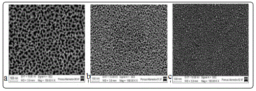
Size of particles, as determined by SEM, is found as 80-190 nm. As seen from SEM images, ZnCdS films shows nano-grain texture, with increasing the pores size from 10 to 30 nm (Figure 1). The size of the grains was different from each other, indicating irregular growth rate of the grains.
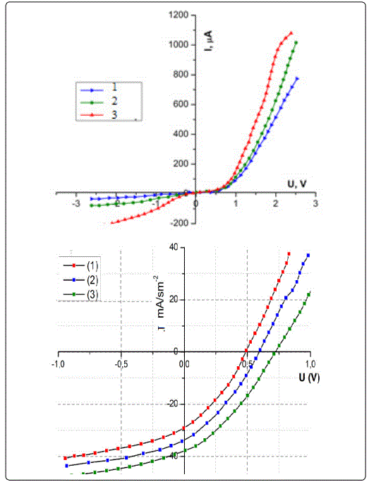
The pass direction corresponds to positive polarity of the external bias on the c-Si layers. Rectification increases from 180 up to 1100, with increasing the pores size from 7.4 to 10 nm.
Further increase in pore sizes leads to sharp decrease of rectification (~12÷15). It is assumed that the change in rectification factor value depending on the pore size is due to the oxygen or nitrogen molecules, because in order to remove excess water from pores and films, hetero junctions were dried in air, just after the deposition (as-deposited hetero junctions).
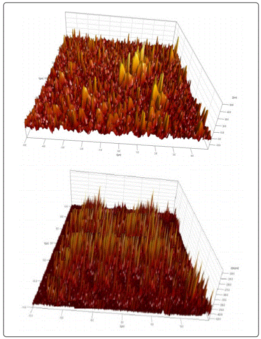
Atomic force microscopy (AFM) is one of the effective ways for the surface analysis of p-Si/10 nm porous-Si/CdS and p-Si/10 nm porous-Si/ZnCdS; thin films due to its high resolution and powerful analysis software (Figure 2).
The effect of preparation conditions of nPS layer such as etching time has very important effect on the photocurrent characteristics of the device, where one can observe from figure 3, that the photocurrent is reduced with the increasing of etching time. This result can be explained since the porosity of nPS layer increases with the increasing of etching time. The increasing of porosity leads to increase the resistivity of nPS layer; therefore, the photocurrent will decrease.
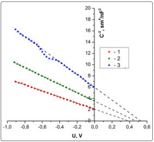
The capacitance-voltage characteristics have been studied in this work. The variation of capacitance as a function of reverse bias voltage in the range of (0-1) V for Nano-ZnCdS/PS hetero junction, which prepared at different etching times (10, 20 and 30) min are shown in Figure 4. It is observed from this figure that the capacitance decreases with increasing the reverse bias. This decreasing was non-linear, that the capacitance becomes constant approximately at high voltages. This behavior is attributed to the increasing in the depletion region width which leading to the increasing of built-in voltage; it is obvious from this Figure that the capacitance at zero bias voltage (Co) decreases with the increasing of etching time of nPS layers. This is attributed to the increase of porosity with the increasing of etching time, which leads to the increasing of the depletion region width and decreasing the capacitance.
The relation between inverse capacitance squared (C-2) against the reverse bias at different values of etching time are shown in (Figure 4). A linear relationship between C-2 and reverse bias voltage was obtained for the structure, this linear relationship represents that the junction was abrupt type. The interception of the straight line with voltage axis at (1/C2 = 0), represents the built-in voltage. Assuming that the resulting junction is one-sided junction, these data were calculated according to Anderson model
In order to explain the reason of this, we investigated the spectral distribution of photocurrent (Jph) depending on the pores size of silicon and morphology of ZnCdS films, in a wavelength range of 300÷1300 nm (Figure 5). It is established that the profile of photocurrent spectrum depends on the pore size and morphology of ZnCdS films. Short wavelength peak for hetero junctions with a pore size of 7.4 nm, is observed at 510 nm, which corresponds to the band gap of CdS films. The films deposited onto the silicon with pore size of 10 nm shows micro-structural morphology, as demonstrated by SEM images.
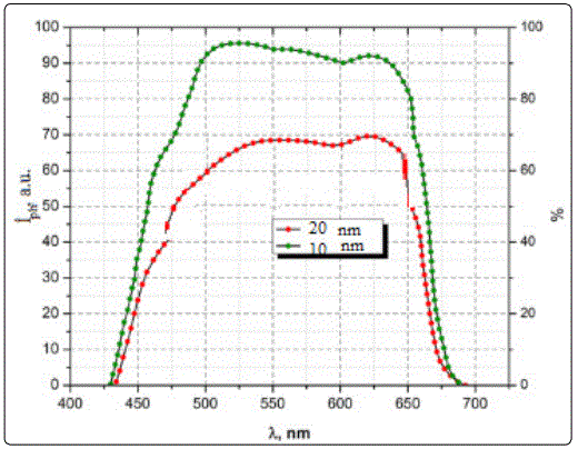
However, long-wavelength peak of spectrum at 1125 nm is due to the direct inter band transitions in c-Si. It can be seen from figure 5, that hetero junctions demonstrate good photo-response in the wavelength range of 510÷ 650 nm. It is assumed that this is due to light absorption in porous silicon. With increasing pores size until 10 nm, shift of peak at 510 nm to the short wavelength region of spectrum is observed, which associated by us with the nano-structural properties of ZnCdS films, i.e. band gap increasing with decrease of crystallite sizes in films. However, an increase of the optical path of light in nano-structured films leads to increase of degree of the light absorption, therefore, hetero junctions with pore sizes of 10 nm, shows greater efficiency compared hetero junctions with pore sizes of 7.4 nm
Conclusion
Nanostructure ZnCdS thin film was fabricated by electro deposition technique. To manufacture the hetero junctions, p-type c-Si wafers of (100) orientation were used as a substrate. Before anodization, the surface of the c-Si substrates were etched in an aqueous solution of HF and further washed in distilled water (at temperature of 80°C and ethyl alcohol and then dried in air. The anodization of c-Si substrate surface was carried out in Teflon chamber with Pt cathode. HF: ethanol solution (1:1) were used for the porous silicon formation. X-ray diffraction patterns exhibit small peaks with a hexagonal phase and the value of average grain size is about 9.603 nm. The current-voltage characteristics of the ZnCdS/PS solar cell under dark conditions show that forward bias current variation approximately exponentially with voltage bias. From the current-voltage characteristics under illumination, the photocurrent increases with the increasing of applied reverse bias voltage and it is reduced with the increasing of etching time. The capacitance for Nano-ZnCdS/PS Solar Cell decreases with the increase of the reverse bias voltage and with the increasing of etching time of nPS layers. That hetero junctions demonstrate good photo-response in the wavelength range of 510 ÷ 650 nm.
References
- Radu M, Ohenescu V, Stan I, et al. Photovoltaic Properties of the CdS/CdTe Hetero junction Solar Cells Before and After Proton Irradiation. Chalcogenide Letters. 2011; 8(8): 477-485.
- Kumar C, Hoa N, Yoon S, Kim E. Highly Photoconductive CdS Thin Films Synthesized by using Chemical Bath Deposition. Journal of Korean Physical Society. 2009; 55(1): 284-287. doi: 10.3938/jkps.55.284
- Perkins C, Hasson F. Surfactant-Assisted Growth of CdS Thin Films for Photovoltaic Applications. J. Vac. Sci. Tech. A Vacuum Surfaces and Films. 2006; 24(3): 497-504. doi: 10.1116/1.2194929
- Patidar D, Sharma R, Jain N, Sharma T, Saxena N. Optical Properties of CdS Sintered Film. Bull. Matt. Sci. 2006; 29(1): 21-24. doi: 10.1007/BF02709350
- Schon H, Schenker O, Battogg B. Solution Processed CdS Thin Film Transistors. Thin Solid Films. 2001; 385(1-2): 271-281. doi: 10.1016/S0040-6090(00)01908-8
- Chavhon S, Bagul S, Patit A, Sharma R. Studies on Structural, Optical and Photoelectron Transportation in Solution Grown Nanosize CdS Thin Films for Photo sensor application. Indian Journal of Engineering & Materials Sciences. 2004; 11:130-136.
- Urbanczyk M, Jakubik W, Maciak E. Sensor Properties of Cadmium Sulphide (CdS) Thin Films in Surface Acoustic Wave System-Preliminary Results. Molecular and Quantum Acoustics. 2005; 26: 273-281.
- Kumar L, Dhawan S, Kumar M, Kamalasanan M, Chandra S. Yellow-Green Organic Light Emitting Diodes Based on Poly (p-phenylene vinylene)/CdS Hetero junction Thin Films. Indian Journal of Pure Applied Physics. 2003; 41(8): 641-645.
- Altaify D, Mahdi Z. Nonlinear Optical Properties of CdS Thin Film Nanoparticles Using z-Scan Technique. Iraqi J. Laser Part A. 2007; 6: 9-14.
- Miredin OC, Choi P, Wuerz R, Raabe D. Atomic-Scale Characterization of the CdS/CuInSe2 Interface in Thin Film Solar Cells. Appl. Phys. Lett. 2011; 98: 103504-103506. doi: 10.1063/1.3560308
- El-Nahass M, A.El-Barry A. Effect of Substrate Temperatures, Deposition Rate and Heat Treatment on Structural and Carrier Transport Mechanisms of Thermal Evaporated p-Cu2s/n-CdS Hetero junction. Indian Journal of Pure & Applied Physics. 2007; 45: 465-475.
- Rakovics V, Horvath ZS, Horvath ZE, Barsony I, Frigeri C, Besagni T. Investigation of CdS/InP Hetero junction Prepared by Chemical Bath Deposition. physica Status Solidi (c). 2007; 4(4): 1490-1493. doi: 10.1002/pssc.200674153
- Kawar S. Chalcogenide Thin Films Having Nanometer Grain Size for Photovoltaic Applications. Research Journal of Chemical Science. 2011; 1(8): 31.
- Oliva A, Rodriguez RC, Canto OS, Sosa V, Quintana P, Pena JL. Comparison of Properties of CdS Thin Films Grown by Two Techniques. Applied Surface Science. 2003; 205: 56-64. doi: 10.1016/S0169-4332(02)01081-4
