

Research Article
Structural, Morphological, and Optical Transitions in Pulsed Laser deposited V2O5–TiO2 Transition Metal Oxide Nanocomposite Thin Films
1FNRL, Department of Physics and Centre for Nanotechnology, IIT Roorkee, India
2CSIR-National Physical Laboratory, Dr. K.S. Krishnan Marg, New Delhi, India
3NanoScience and Technology Center, University of Central Florida, USA
*Corresponding author: Davinder Kaur, FNRL, Department of Physics and Centre for Nanotechnology, IIT Roorkee, India, Tel: 91-1332-2285407, Fax: 91-1332-273560, E-mail: dkaurfph@iitr.ernet.in
Received: March 30, 2018 Accepted: April 10, 2018 Published: April 16, 2018
Citation: Goyal V, Singh P, Choudhary N, Kaur D. Structural, Morphological, and Optical Transitions in Pulsed Laser deposited V2O5–TiO2 Transition Metal Oxide Nanocomposite Thin Films. Madridge J Nanotechnol Nanosci. 2018; 3(1): 90-95. doi: 10.18689/mjnn-1000117
Copyright: © 2018 The Author(s). This work is licensed under a Creative Commons Attribution 4.0 International License, which permits unrestricted use, distribution, and reproduction in any medium, provided the original work is properly cited.
Abstract
We studied the influence of titanium dioxide (TiO2) concentration on the structural and optical properties of vanadium pentoxide (V2O5) thin films deposited on amorphous glass substrate using pulsed laser deposition technique. TiO2 doping into V2O5 matrix revealed an interesting morphological change from an array of high density pure V2O5 nanorods (~140 nm) to granular structure inTiO2-doped V2O5 thin films. The results showed a significant improvement in the transmittance and refractive index in TiO2 doped V2O5 thin films.
Keywords: Pulsed laser deposition; Nanocomposite thin films; Structural properties; Optical properties.
Introduction
The transition metal oxides attract a lot of attention due to their interesting physical, chemical, electronic, and optical properties which arise from the narrow d states as well as their hybridization with the ligand p orbital. The vanadium pentoxide (V2O5) has attracted considerable interest owing to their multivalency, layered structure, wide optical band gap, good chemical and thermal stability, and excellent thermoelectric property [1-3]. Scientific and technological applications of V2O5in thin films form includes electronic and optical switches [4], electro chromic devices [5], window for solar cell [6,7], microelectronic devices [8], thin film batteries (TFB) [9]. V2O5 crystallizes with an orthorhombic unit cell structure and belongs to Pmmn space group with the lattice parameters a=11.51Å, b=3.56 Åand c= 4.3Å [10]. It is fundamentally comprised of VO5 pyramids which form alternating double chain along the b-axis. Alternating double chains of pyramids up/pyramids-down are connected laterally by bridging oxygen to form a sheet or zig-zag ribbon in the a-b plane. The planes themselves are connected by Vander Waals bonds and this looser bonding creates easy cleavages along these planes. This results in VO6 units with three principal V-O distances, which are 1.58Å (along the c-direction); 1.77-2.02Å (bridging oxygen in the basal planes) and 2.79Å (weak bonds in between the layers).The long vanadyl bonds normal to the a-c plane allows mica like cleavage parallel to that plane. V2O5 is an indirect semiconductor with a band gap of 2.3-2.4 eV, which stems from the split-off oxygen 2p band up to vanadium 3d band. Electronic conduction in V2O5 is highlyanisotropic with conduction within the a-b planes considerably higher than conduction perpendicular to these planes.
Understanding the unique properties of V2O5 requires a great structural investigation especially in case of doping the oxide with other elements that may result in a change of morphology, structural arrangement and optical properties of this material. The structural stability of this V2O5 doped with guest atoms is also important because small amount of admixtures may strongly affect the reactivity of this oxide. The novel technology of the nanostructure material assembling provides the possibility of tailoring such materials with unique microstructure properties. The proper amount of transition metal doping could lead to optimal degree of non-stoichiometry for better performance. Since composites and mixed phases can have different properties than their constituent phases. Various metals like W, Pd, Mo, Mn have been used to dope the V2O5 for several applications like enhanced electrochemical performance, better intercalation property, improved cyclic stability, and various other electronic applications. But doping with Titanium dioxide (TiO2) may significantly improve the photo catalytic applications of V2O5. TiO2 has been proven to be an effective material for applications such as photocatalysis [11], dye sensitized solar cells [12], self-cleaning/antifogging surface coatings [13], etc. Its photo catalytic activity is normally determined by the particle size [14], phase composition [15], and the position of the conduction and valance bands in the energy scale [16]. In the thin film form, TiO2 is usually used in photovoltaic applications such as photo electrochemical system (PEC) and dye sensitized solar cell (DSSC) for photon harvesting [17]. Moreover, TiO2 offers the advantage of energy alignment between the energy position of the valance band edge and the redox species in the electrolyte by potential biasing the photo anodes. This helps to optimize the quantum efficiency. The deviation of stoichiometry suggests that the properties of the films are mainly dependent on the deposition technique and the deposition conditions such as vacuum, deposition temperature, deposition rate, residual gases in the vacuum chamber during deposition, etc.
Many research groups have reported work on V2O5 - TiO2 composite thin films [18,19]. These materials have already proved to be promising for the development of the solar energy devices such as counter electrodes for the electro chromic windows and thin film layers for the antireflective filters. The aim of the present study was to synthesize high quality V2O5, TiO2 and (V2O5)100-x–(TiO2)x composite thin films on glass substrate using pulsed laser deposition technique and to study the effect of TiO2 content on the microstructure and optical properties of V2O5.It was observed that doping with TiO2significantly promotes the phase transformation in V2O5from anatase to rutile phase with significant change in morphology from a nanorod array to granular structure. The influence of TiO2 doping on the optical properties of V2O5 films was also discussed.
Experimental Details
For the deposition of pure V2O5, TiO2, and V2O5-TiO2 composite films (TiO2 content from x= 0 to x= 100), 1-inch circular targets of these materials were prepared by the conventional solid-state reaction method. High purity V2O5 and TiO2 powders were thoroughly mixed and calcined at 400°C and 1100°C respectively for 6 h in air. After calcination, V2O5 and TiO2 powders were pressed into pellets and sintered at 650°C for 12 h and 1400°C for 4 h in air respectively. These target materials along with cleaned glass substrates were mounted in a pulsed laser deposition chamber followed by vacuum pumping to a base pressure of 10-6Torr. The targetto-substrate distance was kept at 40 mm and substrates were heated to a temperature of 400°C. For thin film deposition, a pulsed laser beam generated by a KrF excimer laser at a wavelength of 248 nm and pulse duration of 25 ns was introduced into the deposition chamber through a quartz window and focused using an optical lens onto the target surface. The laser fluence on the target was 2-3 J/cm2, while the repetition rate was fixed at 8 Hz. Before target ablation, pure oxygen was introduced and maintained at a pressure of 50 mTorr. Before every deposition, the target was pre-ablated for 2 min in order to ascertain the same state of the target in every deposition. The target holder was scanned in X-Y direction for uniform erosion of the target material. A post deposition annealing at 600°C for 30 min was performed after deposition.
Structural characterization of the films was carried out using a Bruker X-Ray of Cu Kα radiation (1.54Å) with the scanning speed of 2θ = 1°/min in the angle range between 10°and 60°. To obtain a profile fitting with good signal, a polycrystalline Si powder was used for instrumental correction. Optical properties of the deposited films were studied using Varian Cary 5000 UV-VIS/NIR spectrometer with specular reflection attachment in the range between 300 nm and 800 nm having wavelength accuracy of ±2 nm and with scan speed 90 nm/min. The microstructure of the films was investigated using field emission scanning electron microscopy (FESEM) with an operating voltage of 20 keV and NTMDT atomic force microscopy (AFM) in semi-contact mode with silicon nitride (Si3N4) tip of 10 nm radius.
Results and Discussion
Structural properties
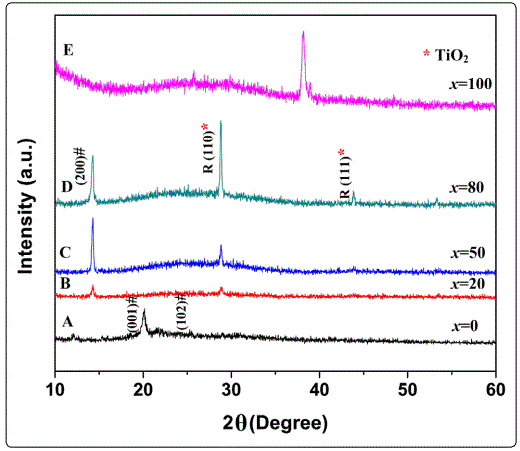
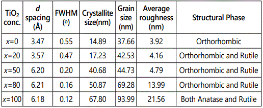
Figure 1 shows the XRD pattern of bulk samples corresponding to pure V2O5, TiO2 and V2O5/TiO2 composite target materials used for the fabrication of nanocomposite films. Figure 2 shows the X-ray diffraction (XRD) pattern of composite (V2O5)100-x–(TiO2)x thin films with different TiO2 content varying from x=0 to x=100.Samples A, B, C, D, and E represents the films with different TiO2 contents, i.e. x=0, x=20, x=50, x=80, and x=100 respectively. Room temperature XRD pattern of pure V2O5 thin film (sample A) deposited at substrate temperature (TS) of 400 °C exhibits peaks at 2θ=13.2°, 19.4° and 25.2°, which are attributed to the Bragg reflections from the (200), (001), and (102) planes, respectively and is indicative of the polycrystalline V2O5 films with orthorhombic crystal structure. It is worth noting that no additional peaks of vanadium oxide phases were present in the XRD pattern, indicating the phase purity of these films. The XRD pattern of composite sample B with TiO2 content (x=20) shows dominant peaks at 14.5° and 28.82°, which corresponds to the (200) reflection from V2O5 and R(110) from TiO2 planes, respectively. When TiO2 content was increased to 50% (sample C), a significant increment in the intensity of both the planes were observed. The intensity of the peaks (200) & R (110) increases with the doping level, due to superior crystalline quality. With further increase in TiO2 content (x =80, sample D) peak at 28.82° (corresponds to rutile TiO2) starts dominating and an additional peak at 44.081° corresponding to rutile TiO2 of plane (111) is observed. It is worth noting that there is no peak corresponding to anatase phase when TiO2 concentration is 50% and 80%. Thus, incorporation of TiO2 in V2O5 leads to formation of rutile phase only.XRD pattern of pure TiO2 (x =100 – sample E) shows peaks at 25.4°, 38.2° and 38.85° which corresponds to the reflections from anatase (101), (004) and rutile (200) respectively. It is observed that in pure TiO2 anatase phase dominates above rutile phase at TS = 400 °C. It could be attributed to different surface free energies associated with different planes. The crystallite size of different samples was estimated using Debye Sherrerʼs formula:
Where λ, θB, and B are the X-ray wavelength (1.54Å), Bragg diffraction angle and line width at half-maximum (FWHM), respectively [20]. The calculated values of crystallite size are
Where λ, θB, and B are the X-ray wavelength (1.54Å), Bragg diffraction angle and line width at half-maximum (FWHM), respectively [20]. The calculated values of crystallite size are depicted in Table 1. Figure 3(a-e) shows the FESEM images of films for samples A-E, respectively. A nanorod formation is clearly evident from the FESEM image of pure V2O5 film. It is because the annealing treatment provides sufficient thermal energy to activate crystallization. The observed nanorods formation can be interpreted as recrystallization process driven by minimization of surface energy. V2O5 has basal {001} planes bonded weakly to each other. The surface energy of the {001} atomic planes is, therefore, smallest because only a limited number of bonds is destroyed when the material is cleaved along these planes. According to the numerical simulation [21], the {001} planes have a value of surface energy of about 0.7 Jm-2, which is significantly smaller than the calculated values for other lower energy surfaces. It is interesting to see that the morphology and the growth mechanism of these V2O5 nanorods are quite similar to those of the formation of zinc oxide nanorods [22]. So, we believe that surface diffusion (migration) plays an important role in the growth process of nanorods.
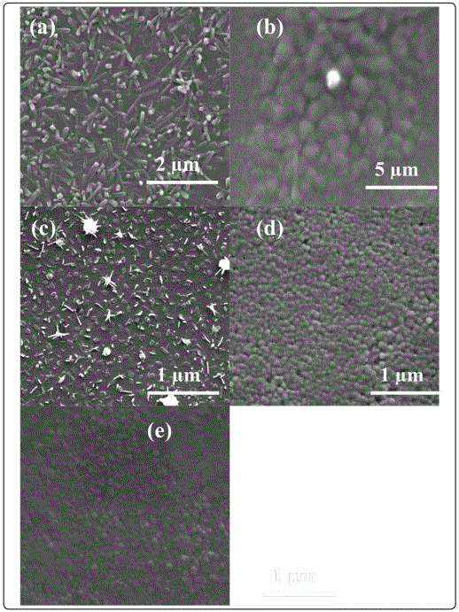
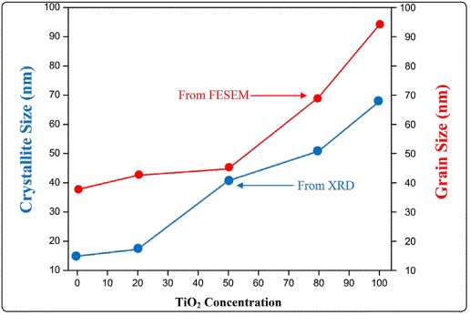
Furthermore, it should be noted that nanorods are not directly formed on glass substrate but on the underlying nanocrystalline V2O5 film. This implies that underlying film act as a nucleation site, with a reduced energy barrier, for the formation of nanorods. Due to annealing at high temperature (TS = 600 °C) the diameter of nanorods increases. It is interesting to note that surface morphology of the films undergoes a transformation from one-dimensional nanorods arrays to two-dimensional film with granular structure after incorporating TiO2 content (20-80%) in V2O5 matrix as shown in Figure 3(a-e). It could be attributed to the fact that in the case of doped systems, the columnar (nanorods type) growth is always inhibited during incorporation of the doping element in to the matrix due to the formation of either defects or aggregation after doping. Thus, for the deposition of composite films, heterogeneous or homogeneous nucleation may occur on the substrate, and the coarsening process (through atomic diffusion) of small particles proceeds with difficulty, in contrast to the undoped V2O5 deposition at the same annealing temperature, due to the presence of TiO2 doping element. Consequently, a granular rather than a columnar structure is formed. Figure 4 shows the crystallite size and grain size of samples calculated by XRD and FESEM analysis. It is worth to note that grain size shown by FESEM is much higher as compared to crystallite size calculated from the XRD results. It could be due to the fact that XRD gives the average mean crystallite size while FESEM showed agglomeration of the grains.
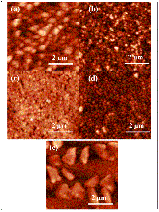
The surface topography of the films as studied by atomic force microscopy (AFM) revealed that laser ablated (V2O5)100-x–(TiO2)x composite thin films were homogenous, smooth and uniform [Figure 5(a-e)]. The average value of surface roughness was found to increase with increasing TiO2 content [Table 1]. The image shows the different grain growth in shape and size with the changing TiO2 content. The occurrence of the large size particles in our film is due to the incomplete elimination of the crater - like features on the target surface, which is caused by ultra-rapid evaporation of the target material. The AFM results are in agreement with the XRD and FESEM results. The film surfaces have no evident defaults such as impurity holes and cracks.
Optical properties
Transmittance and absorbance measurements
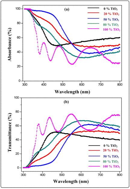
The spectral variations of absorption and transmission for the (V2O5)100-x–(TiO2)x composite thin films deposited onto glass substrate, with different TiO2compositionwere measured over the wavelength range of 300–800 nm and are shown in [Figure 6(a&b)]. At x=0 (pure V2O5), films show transmittance up to50% in the visible range of electromagnetic spectrum. Lack of oscillations suggests that the films so formed are very thin. At x=50 [Figure 6(b)], transmittance is 60%.With the incorporation of TiO2 there is gradual increase in transmittance as addition of TiO2 leads to transparency of films which in turn leads to increase in transmittance. When x=100 [Figure 6(b)], films shows four to five fringes and there is a gradual increase of transmittance towards longer wavelength. It is remarkable that a gradual increase in the red-shift is observed with increase in TiO2 doping. Optical results are in confirmation with AFM and FESEM results. The pure V2O5 films have uniform yellow colour. Such yellow colour indicate that vanadium was incorporated as V+5 in V2O5 lattice, because it is known that V+4 presents a brown and black colour [23].
Refractive index (n) was estimated from the transmission spectrum by using envelope method [24] and following expressions was used to calculate the refractive index


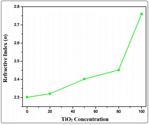
Where n0 is the refractive index of air, n1 is the refractive index of substrate, Tmax and Tmin are maximum and minimum transmittance values at the same wavelength. The calculated value of the refractive index for all the deposited thin films was found to be in the range from 2.30 to 2.76 as shown in the Table 1. Figure 7 shows the change in refractive index with the variation of TiO2 content. For each value of refractive index, different applications can be proposed by variation in TiO2 content doped in V2O5 thin films.
Knowing the refractive index (n), thickness (t) of the films was determined by using the following expression.
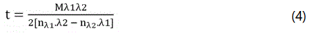
Where M is the number of oscillations between the two extrema and the value of M is equal to 1 between two consecutive maxima and minima, λ1, nλ1 and λ2, nλ2 are the corresponding wavelength and indices of refraction [24]. By using the above relation, the thickness of the film was found ~ 325nm.
Conclusion
In summary, pure V2O5, TiO2 and (V2O5)100-x–(TiO2)x composite thin films were fabricated on amorphous glass substrate at the substrate temperature of 400°C using pulsed laser deposition technique. XRD results revealed polycrystalline nature of undopedV2O5 thin films. SEM results showed the formation of nanorods with the size of ~ 140nm. The formation of granular particles (of few nanometres in size) from nanorods results from either defects or aggregation of particles after doping or due to the coarsening process of small particles. AFM results showed homogeneous, uniform, smooth and crack-free composite films. The TiO2 content was found to have a significant impact on the transmittance and refractive index of the films. The transmittance was significantly improved from 56% to 71%with the incorporation of TiO2. The film colouration is found to have stable over several tens of hours claiming high colouration memory. TiO2doped V2O5 films could play an important role in various photo catalytic, electro chromic and antireflective coatings applications.
Acknowledgements
VG is thankful to MHRD, India for the award of assistantship for M. Tech dissertation. NC acknowledges the University Grants Commission, India for the award of Junior Research Fellowship during his Ph.D.
References
- Ramana CV, Hussain OM, Srinivasalu NB, Julien C, Balkanski M. Physical investigations on electron-beam evaporated vanadium pentoxide films. Mater SciEng B. 1998; 52(1): 32-39. doi: 10.1016/S0921-5107(97)00273-0
- Fujita Y, Miyazaki K, Tatsuyama C. On the Electrochromism of evaporated V2O5 films. Jpn J Appl Phys. 1985; 24(1): 1082. doi: 10.1143/JJAP.24.1082
- Moshfegh AZ, Ignatiev A. Formation and characterization of thin film vanadium oxides: Auger electron spectroscopy, X-ray photoelectron spectroscopy, X-ray diffraction, scanning electron microscopy, and optical reflectance studies. Thin Solid Films. 1991; 198(1-2): 251-268. doi: 10.1016/0040-6090(91)90344-W
- Colton RJ, Guzman AM, Rabalais JW. Electrochromism in some thin-film transition-metal oxides characterized by x-ray electron spectroscopy. J. Appl. Phys. 1978; 49: 409. doi: 10.1063/1.324349
- Wei Y, Zhou J, Zheng J, Xu C. Improved stability of electrochromic devices using Ti-doped V2O5 film. Electrochim Acta. 2015; 166: 277-284. doi: 10.1016/j.electacta.2015.03.087
- Alamria SN, Joraid AA. Smart windows with different thicknesses of V2O5 as ion storage layers. Materials Science Forum. 2011; 663-665: 743-750. doi: 10.4028/www.scientific.net/MSF.663-665.743
- Dultsev FN, Vasilieva LL, Maroshina SM, Pokrovsky LD. Structural and optical properties of vanadium pentoxide sol-gel films. Thin Solid Films. 2006; 510(1-2): 255-259. doi: 10.1016/j.tsf.2005.12.264
- Armstrong E, McNulty D, Geaney H, OʼDwyer C. Electrodeposited structurally stable V2O5 inverse opal networks as high performance thin film lithium batteries. ACS Appl. Mater. Interfaces. 2015; 7(48): 27006-27015. doi: 10.1021/acsami.5b09511
- Yoon YS, Kim JS, Choi SH. Structural and electrochemical properties of vanadium oxide thin films grown by d.c. and r.f. reactive sputtering at room temperature. Thin Solid Films. 2004; 460(1-2): 41-47. doi: 10.1016/j.tsf.2004.01.075
- Nakata K, Fujishima A. TiO2 photocatalysis: Design and applications. J. Photochem. Photobiol. C. 2012; 13(3): 169-189. doi: 10.1016/j.jphotochemrev.2012.06.001
- Fan J, Li Z, Zhou W, et al. Dye-sensitized solar cells based on TiO2 nanoparticles/nanobelts double-layered film with improved photovoltaic performance. Appl Surf Sci. 2014; 319: 75-82. doi: 10.1016/j.apsusc.2014.07.054
- Lai Y, Tang Y, Gong J, et al. Transparent superhydrophobic/superhydrophilic TiO2-based coatings for self-cleaning and anti-fogging. J. Mater. Chem. 2012; 22: 7420-7426. doi: 10.1039/C2JM16298A
- Tan Z, Sato K, Takami S. Particle size for photocatalytic activity of anatase TiO2 nanosheets with highly exposed {001} facets. RSC Adv. 2013; 3: 19268-19271. doi: 10.1039/C3RA43383H
- Balázs R., Major Z, Szarka D, et al. Influence of TiO2 phase composition on the photocatalytic activity of TiO2/MWCNT composites prepared by combined sol-gel/hydrothermal method. J Mol Catal A: Chem. 2016; 414: 140-147. doi: 10.1016/j.molcata.2016.01.016
- Yan H, Wang X, Yao M, Yao X. Band structure design of semiconductors for enhanced photocatalytic activity: The case of TiO2. Progress in Natural Science: Materials International. 2013; 23(4): 402-407. doi: 10.1016/j.pnsc.2013.06.002
- Deb SK. Dye-sensitized TiO2 thin-film solar cell research at the National Renewable Energy Laboratory (NREL). Solar Energy Materials & Solar Cells. 2005; 88: 1-10. doi: 10.1016/j.solmat.2004.09.007
- Kim S, Taya M. Electrochromic windows based on V2O5–TiO2 and poly (3,3-dimethyl-3,4-dihydro-2H-thieno[3,4-b][1,4]dioxepine) coatings. Solar Energy Materials and Solar Cells. 2012; 107: 225-229. doi: 10.1016/j.solmat.2012.06.032
- Patterson AL. The scherrer formula for X-Ray particle size determination. Phys. Rev. 1939; 56: 978. doi: 10.1103/PhysRev.56.978
- Sayle DC, Gay DH, Rohl AL, et al. Computer modeling of V2O5: surface structures, crystal morphology and ethane sorption. J. Mater. Chem. 1996; 6: 653-660. doi: 10.1039/jm9960600653
- Yan X, Li Z, Chen RQ, Gao W. Template growth of ZnO nanorods and microrods with controllable densities. Cryst. Growth Des. 2008; 8(7): 2406-2410. doi: 10.1021/cg7012599
- Melghit K, Pillai SP, Das VGK. Preparation of Vanadium Tin Oxide Solid Solution at 500°C from Xerogel and Metallic Tin. J. Mater. Sci. lett. 1999; 18(9): 661-663. doi: 10.1023/A:1006619523123
- Manifacier JC, Gasiot J, Fillard JP. A simple method for the determination of the optical constants n, k and the thickness of a weakly absorbing thin film. J. Phys. E: Sci. Instrum. 1976; 9(11): 1002. doi: 10.1088/0022-3735/9/11/032
