
Research Article
Electronic & Optical properties of Transition-Metal Dichalcogenides
Interdisciplinary Program in Materials Science & Engineering, New Jersey Institute of Technology, Newark, USA
*Corresponding author: Nuggehalli M. Ravindra, Interdisciplinary Program in Materials Science & Engineering, New Jersey Institute of Technology, Newark, USA, E-mail: nmravindra@gmail.com
Received: June 15, 2017 Accepted: July 3, 2017 Published: July 8, 2017
Citation: Tang W, Rassay SS, Ravindra NM. Electronic & Optical properties of TransitionMetal Dichalcogenides. Madridge J Nanotechnol Nanosci. 2017; 2(1): 58-64. doi: 10.18689/mjnn-1000111
Copyright: © 2017 The Author(s). This work is licensed under a Creative Commons Attribution 4.0 International License, which permits unrestricted use, distribution, and reproduction in any medium, provided the original work is properly cited.
Abstract
Transition-metal dichalcogenides (TMDCs) have emerged as a new class of semiconductors that display distinctive properties at the monolayer thickness. Their electronic and optical properties are of particular interest and importance for applications in optoelectronics as light emitters, detectors, and photovoltaic devices. In the first part of this study, the temperature dependence of the energy gap of TMDCs (MoS2, MoSe2, WS2 and WSe2) for monolayers is discussed. The second part focuses on the determination and analysis of the spectral properties of these materials, at monolayer and bulk, in the range of 1.5-3.0 eV by MATLAB simulations. The optical bandgaps of TMDC monolayers have been simulated from their spectral dependence of the absorption coefficient. Case studies of the simulation of the optical properties of these materials on silicon, gold and fused silica substrates are presented.
Keywords: Transition Metal Dichalcogenides; Electronic Properties; Optical Properties; Influence of Substrates; Bandgap; Temperature Dependence; Band Structure.
Introduction
In recent years, the layered transition metal dichalcogenides (TMDCs) i.e. MX2 (M= Mo and W; X= S and Se) have attracted unprecedented attention due to their unusual properties that has been attributed to their two-dimensional (2D) structure and high crystal quality, leading to significant research interest. Unlike graphene, these materials have an intrinsic band-gap which makes them suitable for transistor channels reminiscent of an ideal switch for digital logic applications [1].
TMDC monolayers such as MoS2, WS2, MoSe2 and WSe2, exhibit a direct band gap. They can be used in electronic devices such as transistors and in optical components as emitters and detectors. The band gaps of TMDC monolayers are in the visible range (between 400 nm and 700 nm). TMDC monolayers are promising materials for applications in optoelectronics [2].
The preliminary studies of these TMDCs have been reported earlier [3]. In the present study, details of the energies of peaks and valleys in the optical spectra of the TMDCs have been identified. This should help to better interpret and understand the band structure of these materials. Values of the energy gap have been estimated for monolayer TMDCs based on the models for the energy dependence of the absorption coefficient.
Electronic Properties of TMDCs
At room temperature, the band gaps of bulk MoS2, MoSe2, WS2 and WSe2 are, respectively, as follows: 0.75eV, 0.80eV, 0.89eV and 0.97eV. For monolayer MoS2, MoSe2, WS2 and WSe2, the corresponding band gaps, respectively, are 1.89eV, 1.58eV, 2.05eV and 1.61eV [4]. The monolayer TMDCs have larger band gap values than those of bulk TMDCs. We utilize these values to compare with their respective optical band gaps which have been simulated in the latter part of this paper.
Except for the lead chalcogenides, PbS, PbSe and PbTe [5], generally, the energy gap of most of the semiconductors is known to decrease with increase in temperature [6]. This is due to the electron-phonon interactions as well as the relative shift in the valence and conduction bands in the semiconductor [7]. One of the approaches to determining the temperature dependence of the energy gap of semiconductors is given by equation (1). Formulated by OʼDonnell [8], the equation serves to be a direct replacement of Varshiniʼs equation [9].
Eg (T) = Eg (0) – S 〈ħω〉 [coth (〈ħω〉/2kBT) - l] (1)
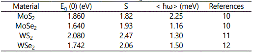
Eg (0) is the band gap at 0 K, S is a dimensionless coupling constant, kB is the Boltzmann Constant and 〈ħω〉 is the average phonon energy. This equation has been explicitly used due to poor fitting results obtained from using full theoretical treatments [7]. Fitting parameters, based on equation (1), are shown in Table I. Monolayer TMDCs are considered in our calculations of the temperature dependence of the energy gap. Due to the sensitivity of semiconductor device properties and their performance to temperature, we have considered such a study of TMDCs. The variation in the band gap of TMDCs with temperature is shown in Figure 1. The results have been implemented using MATLAB with equation (1).
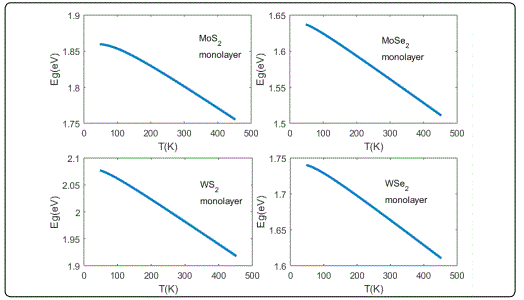
As observed in Figure 1, the energy gap decreases with increase in temperature, which is generally the case for most semiconductors [6].
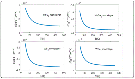
As can be seen in Figure 2, (dEg/dT) of the monolayer TMDCs is non-linear with temperature and is negative. It decreases with increase in temperature.
Optical Properties
In recent years, there has been a large volume of research conducted on the optical properties of TMDCs. However, much of the research revolves around the spectral reflectance, differential reflectance, differential transmittance, spectral absorptance and absorbance. These studies are usually based on experimental research and very less or, in some cases, no simulations are carried out. Despite the intense research carried out on the optical properties of TMDCs, most of the studies do not give a definite value of refractive indices and extinction coefficients. Furthermore, the results of most of the studies involving reflectance, absorptance and transmittance calculations are not in accordance with each other and there is a large spread in the obtained data of the optical properties of TMDCs.
In our work, we have determined the values of optical constants (n and k) and optical properties (R, T and A) by MATLAB simulations under conditions of normal incidence. Li et. al [13]. have reported their studies of the dielectric constants for monolayer TMDCs at room temperature (ε1 and ε2) from experimental reflectance spectra by a constrained Kramers-Kronig analysis; we have utilized these values to calculate the photon energy-dependent refractive index (n) and extinction coefficient (k). As reported by Mukherjee et. al [14], the values of n and k determined by Li et. al [13], are found to be better than the set of values determined by other authors. Hence, we have chosen the data of the optical properties, reported by Li et. al [13] in the present study.
In order to elucidate the influence of the substrates on the optical properties, three different substrates, silicon, gold and fused silica wafers, of 650μm (equal) thickness, have been used in the simulation of the optical properties. These simulations have been performed in order to study the variation in the optical properties of TMDCs on a representative semiconductor, metal and insulator substrate which could contribute to their understanding and facilitate the applications of this multilayer system in areas such as coatings, electronics, optoelectronics, sensors, circuits and systems.
All the calculations of the optical properties in the present work are carried out at room temperature and under conditions of normal incidence. The complex dielectric constant (εr = ε1 + iε2) is a function of the amount of light absorbed by a material; ε1 and ε2 are, respectively, the real and imaginary parts of the complex dielectric constant; these are related to the refractive index and extinction coefficient by the following equations:
ε1 = n2 - k2 (2)
ε2 = 2nk (3)
Here, n and k are the refractive index and extinction coefficient of the material, respectively.
From equations (2) and (3), we get:
4n4 - 4n2ε1 - ε22 = 0 (4)
k = (ε2/2n) (5)
By solving equation (4), we obtain multiple values of n; we choose the real and positive value of n to obtain the value of the extinction coefficient k from equation (5).
In these simulations, monolayer thickness of MoS2 and WS2 are considered as 0.65nm [15], while monolayer thickness of MoSe2 and WSe2 are taken as 0.70nm [15]. The bulk thickness of all the TMDCs are taken as 20nm, which seems to be the optimal value for the TMDCs [12].
Under conditions of normal incidence, the wavelength dependent Reflectance (R), Transmittance (T) and Absorptance (A) are given by:
R = [(n-1)2+k2] / [(n+1)2+k2] (6)
T = (1-R) (e-αt) (7)
In equation (7), α is the absorption coefficient and is calculated from equation (8).
α = (4πk/λ) (8)
Here, k is the extinction coefficient of the TMDC and λ is the wavelength (in nm) of the photon incident on the TMDC material.
A = (1 – R – T) (9)
The above calculations have been performed for suspended monolayer and bulk TMDCs and are dependent on the incident photon energy and thickness of the material.
Equation (10) is used to compute the reflectance of the TMDCs on silicon, gold and fused silica substrates:
R = [(n1-n2)2+k12] / [(n1+n2)2+k12 (10)
where, n1 and k1 are the refractive index and extinction coefficient of the TMDC, respectively, and n2 is the refractive index of the substrate. The transmittance and absorptance calculations for double layer follow the conventional phenomenological approach. The interface at the double layer is considered to be abrupt (no mixing or roughness at the interface is considered in these calculations).
Optical constants, n and k, are determined initially, following which the optical properties of suspended monolayer and bulk TMDCs are computed. Similarly, the optical properties of monolayer and bulk TMDCs on silicon, gold and fused silica substrate are determined.
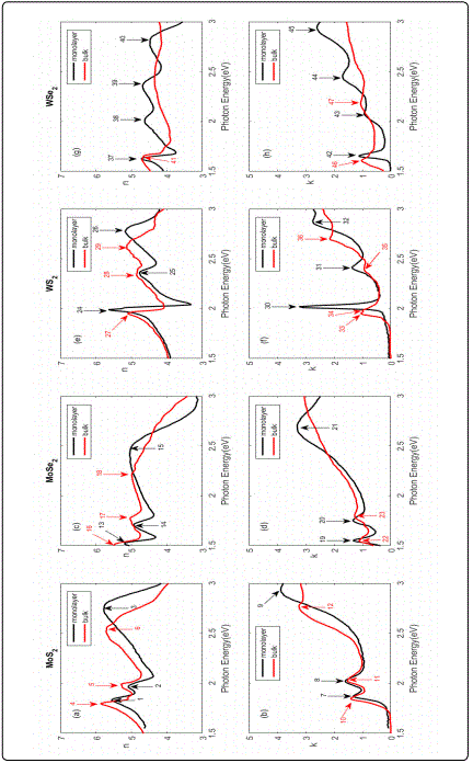
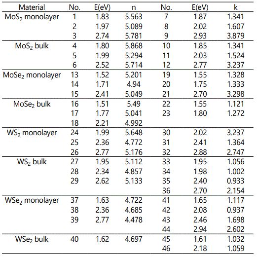
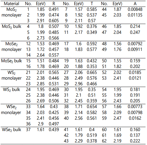
Figure 3 shows the simulated n and k values of monolayer and bulk TMDC. In Figure 3, the peaks are attributed to the A and B exciton absorptions respectively. There is an observed shift in the values of n for monolayer and bulk TMDCs; this could be attributed to the difference in A and B exciton energy in bulk and monolayer TMDCs. The maximum value of refractive index (n) and the corresponding energy (E) for monolayer MoS2, MoSe2, WS2 and WSe2 are as follows: 5.78(2.74eV), 5.20(1.52eV), 5.64(1.99eV) and 4.72(1.63eV) respectively.
Similarly, the maximum value of n for bulk MoS2, MoSe2, WS2 and WSe2 and the corresponding energy (E), respectively, are 5.86(1.80eV), 5.49(1.51eV), 5.13(2.62eV) and 4.69(1.62eV). The difference in the maximum values of n between monolayer and bulk is significant and hence we can conclude that a change in the thickness of the material affects the refractive index. These values are in agreement with the values reported by Zhao et. al [16] and are very close to the values presented by Liu et. al [17]. In addition, the energies corresponding to the maximum refractive index differ significantly between the bulk and the monolayer.
The maximum value of extinction coefficient (k) and the corresponding energy (E) for monolayer MoS2, MoSe2, WS2 and WSe2 are, respectively, as follows: 3.87(2.93eV), 3.29(2.70eV), 3.23(2.02 eV) and 2.60(2.94eV). Similarly, the maximum value of k and the corresponding energy (E) for bulk MoS2, MoSe2, WS2 and WSe2 are, respectively, 3.23(2.77eV), 3.04(3.00eV), 2.42(3.00eV) and 1.56(3.00eV). The difference in the maximum values of k between monolayer and bulk is significant and hence we can conclude that a change in the thickness of the material significantly affects the extinction coefficient. It should be noted that the above analysis is based on the range of photon energies, 1.5 to 3.0 eV, considered in this study. The energies corresponding to the features in the variations of n and k, with energy, for monolayer and bulk TMDCs are summarized in Table II.
The nature of the bandgap, direct or indirect, is generally determined by the absorption spectra [18, 19]. While a variety of approaches to the determination of energy gap of semiconductors have been detailed in the literature, the various functional forms of the spectral dependence of the absorption coefficient have been utilized to determine the value of the band gap as well as its nature – direct or indirect. If a plot of α2 versus ħν leads to a straight line, it is inferred as a direct band gap. The band gap is evaluated by extrapolating the α2 versus ħν straight line to α = 0 axis. However, a plot of α1/2 versus ħν, leading to a straight line, is inferred as an indirect band gap. This indirect band gap is estimated by extrapolating the α1/2 versus ħν straight line to α = 0 axis.
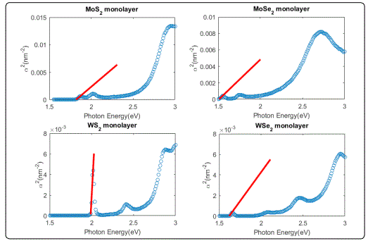
A similar analysis for monolayer TMDCs is shown utilizing our simulated absorption coefficient values. As seen from Figure 4, we observe a straight line corresponding to the first peaks of all the four monolayer TMDCs; this shows that the monolayer TMDCs have direct band gaps. The values of the optical band gap of monolayer TMDCs were obtained by solving the equations to the straight lines. The optical band gaps of monolayer MoS2, MoSe2, WS2 and WSe2 are 1.82 eV, 1.51 eV, 1.98 eV and 1.62 eV, respectively. The calculated optical band gaps are generally smaller than the electronic band gaps; this is due to the additional energy absorbed by the electrons during the transition from the valence band to the conduction band; there is a difference in the coulomb energies of the two systems (excitation spectroscopy and tunneling spectroscopy) which therefore causes changes in the optical band gaps and electronic band gaps.
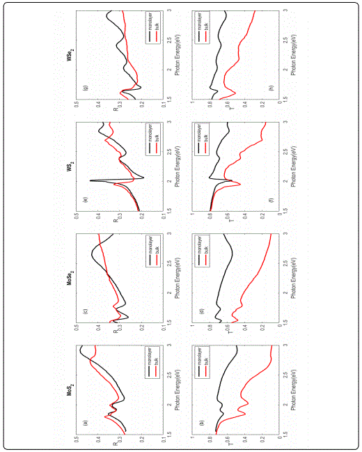
The simulated reflectance and transmittance spectra, under conditions of normal incidence and room temperature, are presented in Figure 5. For all four monolayer and bulk TMDCs, the two lowest energy peaks in the reflectance spectra correspond to the excitonic features that are associated with the inter-band transitions in the K (Kʼ) point in the Brillouin zone [20]. The two significant peaks in Figure 5 can be attributed to the splitting of the valence bands by spin orbit coupling [21]. At higher photon energies, we observe the spectrally broad response from higher-lying inter-band transitions [20], including the transitions near the Γ point [22, 23]. The maximum value of Reflectance (R) and the corresponding energy (E) for monolayer MoS2, MoSe2, WS2 and WSe2 are, respectively, as follows: 60.5% (2.91eV), 55.7% (2.64eV), 56.5% (2.01eV) and 49.7% (2.90eV). Similarly, the maximum value of R for bulk MoS2, MoSe2, WS2 and WSe2 are, respectively, as follows: 56.6% (2.73eV), 52.6% (2.98eV), 50.6% (2.69eV) and 43.9% (1.61eV).
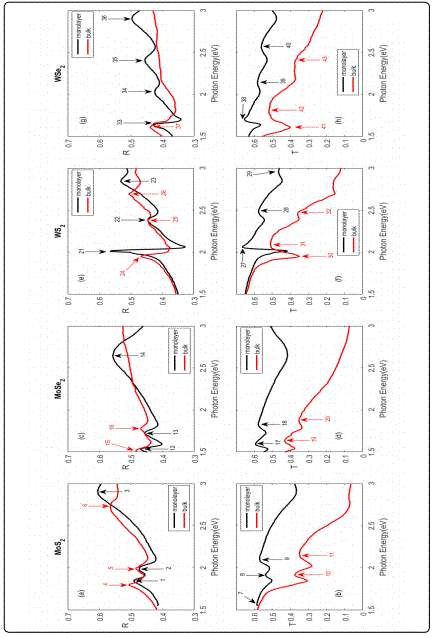
For the simulated transmittance spectra, the maximum values of Transmittance (T) and the corresponding energy (E) for monolayer MoS2, MoSe2, WS2 and WSe2 are, respectively, as follows: 57.0% (2.11eV), 59.2% (1.60eV), 66.5% (2.06eV) and 65.4% (1.71eV). The maximum value of T for bulk MoS2, MoSe2, WS2 and WSe2 are, respectively, 58.2% (1.50eV), 43.1% (1.63eV), 64.5% (1.50eV) and 55.6% (1.50eV).
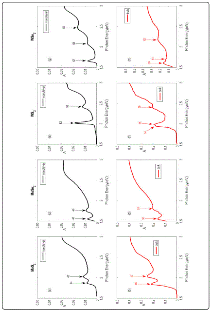
The simulated absorptance spectra are shown in Figure 6. Spectra of monolayer and bulk are separated due to the large change in magnitude of absorptance of monolayer and bulk. This change is reasonable due to the increase in the number of layers which leads to increase in absorptance of light by the material. As observed from Figure 6, the maximum values of Absorptance (A), in the energy range of 1.5 to 3.0 eV, for monolayer MoS2, MoSe2, WS2 and WSe2, occur at 3eV and are, respectively, as follows: 2.93%, 2.78%, 2.55% and 2.72%. Similarly, the maximum values of A for bulk MoS2, MoSe2, WS2 and WSe2 also occur at 3eV and are, respectively, as follows: 39.1%, 40%, 39.7% and 34.87%. The location of the peaks in either case remains relatively similar; these peaks are the A and B exciton absorption peaks which originate from the spin-split direct gap transitions at the K point of the Brillouin zone. All the energy values corresponding to the features, present in Figure 5 and Figure 6, are summarized in Table III.
Optical properties of monolayer and bulk TMDCs on three representative substrates, gold, silicon and fused silica, have been simulated. The values of n and k for gold, silicon and fused silica have been used from an open source website [24]. These three substrates are chosen, in this study, due to their wide applications in the semiconductor industry.
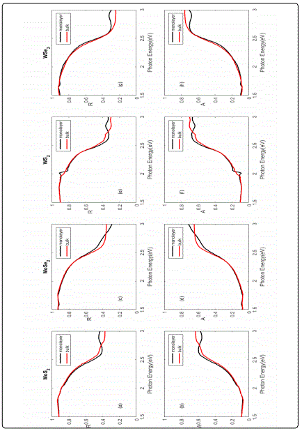
Figure 7 shows the simulated reflectance and absorptance spectra of TMDC/Au. We observe that the reflectance tends to decrease with increase in photon energy, while the absorptance of TMDC/Au increases with the increase in photon energy. Due to the large thickness of gold considered in the simulations, the transmittance of TMDC/Au is ~0 in this energy range; thus, reflectance and absorptance are complementary with each other. We also observe that the change in thickness of TMDC does not necessarily cause a significant change in the reflectance and absorptance of the TMDC/Au. No sharp peaks are observed in the reflectance and absorptance spectra. Maximum values of reflectance and absorptance for monolayer TMDC/Au and bulk TMDC/Au remain approximately the same, with maximum reflectance of ~90% and maximum absorptance of ~70%. It is to be noted within this context that, for the wavelength range considered in this study, the transmittance of gold is ~0 for thickness of 0.1 microns.
The simulated reflectance spectra of TMDC/Si are presented in Figure 8. As observed from this figure, the maximum values of Reflectance (R) for monolayer MoS2, MoSe2, WS2 and WSe2 on silicon are, respectively, as follows: 15.16%, 14.76%(2.84eV), 13.15% and 10.84%. Similarly, the maximum value of R for bulk MoS2, MoSe2, WS2 and WSe2 on silicon are 12.33%, 14.94%, 7.78% and 3.80%, respectively.
The maximum value of Absorptance (A) for monolayer MoS2, MoSe2, WS2 and WSe2 on silicon are as follows, respectively: 98.81%(1.58eV), 98.2%(1.61eV), 99.92% and 99.84%(1.73eV). The maximum value of A for bulk MoS2, MoSe2, WS2 and WSe2 on silicon are 98.6%, 97.6%(1.62eV), 99.87% and 99.44%(1.90eV), respectively.
The reflectance has a very low value with the average maximum value of ~10% as compared to that of TMDC/Au (average maximum value of ~90%). The absorptance of TMDC/Si is very high compared to that of TMDC/Au. Similar to TMDC/Au, the transmittance of TMDC/Si is ~0 due to the large thickness of the silicon wafer and is therefore not included in this study.
Figure 9 presents the simulated reflectance and transmittance spectra of monolayer and bulk TMDCs/fused silica. It is observed that the transmittance of TMDC/fused silica is considerably high which is due to the transparent nature of fused silica and TMDCs. As observed from Figure 9, the maximum value of Reflectance (R) for monolayer MoS2, MoSe2, WS2 and WSe2 on fused silica are as follows: 48.06%(2.91eV), 42.74%(2.65eV), 43.60%(2.01eV) and 35.94%(2.90eV), respectively. The maximum value of R for bulk MoS2, MoSe2, WS2 and WSe2 on fused silica are: 43.48%(2.73eV), 39.41%(3.00eV), 35.97%(2.71eV) and 29.76%(1.61eV), respectively.
The maximum value of Transmittance (T) for monolayer MoS2, MoSe2, WS2 and WSe2 on fused silica are, respectively, as follows: 72.81%(1.57eV), 73.37%(1.60eV), 80.26%(2.07eV). The maximum value of T for bulk MoS2, MoSe2, WS2 and WSe2 on fused silica at 1.50eV, are 72.48%, 54.75%, 78.64% and 68.86%, respectively.
Simulated absorptance spectra of TMDC on fused silica are shown in Figure 10. The maximum values of Absorptance (A) for monolayer MoS2, MoSe2, WS2 and WSe2 on fused silica are as follows: 3.83%, 3.57%, 3.26% and 3.43%, respectively. The maximum values of A for bulk MoS2, MoSe2, WS2 and WSe2 on fused silica are 50.33%, 51.06%, 50.40% and 43.7%, respectively.
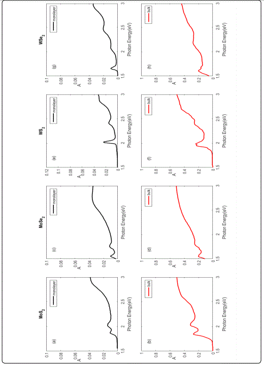
The absorptance spectra shown in Figure 10 are very similar to that in Figure 6; however, the values differ from each other by a small factor. The trend in the change in the value of the absorptance for monolayer and bulk TMDCs are similar.
Conclusion
In the above study, an overview of the electronic and optical properties of transition metal dichalcogenides (MoS2, MoSe2, WS2 and WSe2) has been presented. Temperature dependence studies of the energy gap of monolayer TMDCs, in the range of 50 to 450 K, have been discussed. The optical constants and optical properties of suspended monolayer and bulk MoS2, MoSe2, WS2 and WSe2 have been simulated by mathematical modeling utilizing MATLAB. The results are in accord with the experimental data and show an appreciable convergence. Based on the absorption coefficient, the optical band gaps of these monolayer TMDCs have been evaluated and compared with their respective electronic band gaps. The calculated optical properties of TMDCs on semiconductor, metal and fused silica substrates are presented.
References
- Mak KF, Lee C, Hone J, Shan J, Heinz TF. Atomically thin MoS2: A new direct gap semiconductor. Physical Rev. Lett. 2010; 105(13): 136805-1. doi: 10.1103/PhysRevLett.105.136805
- Splendiani A, Sun L, Zhang Y, et al. Emerging photoluminescence in monolayer MoS2. Nano Lett. 2010; 10(4): 1271-75. doi: 10.1021/nl903868w
- Kumar A, Ahluwalia PK. Electronic structure of transition metal dichalcogenides monolayers 1H-MX2 (M = Mo, W; X = S, Se, Te) from ab-initio theory: new direct band gap semiconductors. The European Physical Journal B. 2012; 85: 186. doi: 10.1140/epjb/e2012-30070-x
- Ravindra NM, Auluck S, Srivastava VK. Temperature dependence of the energy gap in PbS, PbSe and PbTe. Physica Status Solidi (a). 1979; 52(2): k151-155. doi: 10.1002/pssa.2210520255
- Ravindra NM, Srivastava VK. Temperature dependence of the energy gap in semiconductors. J. Phys. Chem. Solids. 1979; 40(10): 791-93. doi: 10.1016/0022-3697(79)90162-8
- OʼDonnell KP, Chen X. Temperature dependence of semiconductor bandgaps. Appl. Phys. Lett. 1991; 58(25): 2924. doi: 10.1063/1.104723
- Varshney YP. Temperature dependence of the energy gap in semiconductors. Physica. 1967; 34(1): 149-54. doi: 10.1016/0031-8914(67)90062-6
- Tongay S, Zhou J, Ataca C, et al. Thermally driven crossover from indirect toward direct bandgap in 2D semiconductors: MoSe2 versus MoS2. Nano Letters. 2012; 12(11): 5576-580. doi: 10.1021/nl302584w
- He Z, Sheng Y, Rong Y, Lee GD, Li J, Warner JH. Layer-dependent modulation of tungsten disulfide photoluminescence by lateral electric fields. ACS Nano. 2015; 9(3): 2740-748. doi: 10.1021/nn506594a
- Arora A, Nogajewski K, Molas M, Koperski M, Potemski M. Exciton band structure in layered MoSe2: from monolayer to the bulk limit. Nanoscale. 2015; 7(23): 10421. doi: 10.1039/C5NR06782K
- Li Y, Chernikov A, Zhang X, et al. Measurement of the optical dielectric function of monolayer transition-metal dichalcogenides: MoS2, MoSe2, WS2 and WSe2. Phys. Rev. B. 2014; 90: 205422-1. doi: 10.1103/PhysRevB.90.205422
- Mukherjee B, Tseng F, Gunlycke D, Amara KK, Eda G, Simsek E. Complex electrical permittivity of the monolayer molybdenum disulfide (MoS2) in near UV and visible. Optical Materials Express. 2015; 5(2): 447-455. doi: 10.1364/OME.5.000447
- Wang Z, Su Q, Yin GQ, et al. Structure and electronic properties of transition metal dichalcogenide MX2 (M = Mo, W, Nb, X=S, Se) monolayers with grain boundaries. Materials Chemistry and Physics. 2014; 147(3): 1068-073.
- Zhao YH, Yang F, Wang J, Guo H, Ji W. Continuously tunable electronic structure of transition metal dichalcogenides superlatticess. Scientific Reports. 2015; 5(1): 8356. doi: 10.1038/srep08356
- Liu HL, Shen CC, Su SH, Hsu CL, Li MY, Li LJ. Optical properties of monolayer transition metal dichalcogenides probed by spectroscopic ellipsometry. Applied Physics Letters. 2014; 105(20): 201905-1. doi: 10.1063/1.4901836
- Ravindra NM, Narayan J, Ance C, Dechelle F, Ferraton JP. Low temperature optical properties of hydrogenated amorphous silicon. Materials Letters. 1986; 4(8-9): 343-49. doi: 10.1016/0167-577X(86)90066-2
- Ravindra NM, Narayan J. Optical properties of silicon related insulators. J. Applied Physics.1987; 61(5): 2017. doi: 10.1063/1.337998
- Wilson JA, Yoffe AD. The transition metal dichalcogenides discussion and interpretation of the observed optical, electrical and structural properties. Adv. Phys. 1969; 18(73): 193-335. doi: 10.1080/00018736900101307
- Mattheiss LF. Band structures of transition-metal-dichalcogenide layer compounds. Phys. Rev. B. 1973; 8: 3719. doi: 10.1103/PhysRevB.8.3719
- Qiu DY, da Jornada FH, Louie SG. Optical spectrum of MoS2: Many-body effects and diversity of exciton states. Phys. Rev. Lett. 2013; 111(21): 216805-1. doi: 10.1103/PhysRevLett.111.216805
- Carvalho A, Ribeiro RM, Castro AH. Band nesting and the optical response of two-dimensional semiconducting transition metal dichalcogenides. Phys. Rev. B. 2013; 88: 115205-1. doi: 10.1103/PhysRevB.88.115205
