

Research Article
A Comparable Study On ZnO-Based Room Temperature Ozone Sensing Characteristics Utilizing Conductometric and Surface Acoustic Waves Techniques
1Department of Physics, University of Crete, Crete, Greece
2Institute of Electronic Structure and Laser (IESL), Foundation for Research and Technology Hellas (FORTH), Crete, Greece
3Crete Center for Quantum Complexity and Nanotechnology, Department of Physics, University of Crete, Greece
*Corresponding author: D. Katerinopoulou, Department of Physics, University of Crete, Crete, Greece, E-mail: dkaterin@iesl.forth.gr
Received: March 9, 2017 Accepted: April 3, 2017 Published: April 10, 2017
Citation: Katerinopoulou D, Moschovis K, Gagaoudakis E, Aperathitis E, Binas V, Kiriakidis G. A Comparable Study on ZnO based Room Temperature Ozone Sensing Characteristics utilizing Conductometric and Surface Acoustic Waves Techniques. Madridge J Nanotechnol Nanosci. 2017; 2(1): 44-51. doi: 10.18689/mjnn-1000109
Copyright: © 2017 The Author(s). This work is licensed under a Creative Commons Attribution 4.0 International License, which permits unrestricted use, distribution, and reproduction in any medium, provided the original work is properly cited.
Abstract
Ozone (O3) detection is of great interest for public safety and human health. In this work, zinc oxide (ZnO) films were tested as sensing elements against different ozone concentrations. The DC Magnetron Sputtering technique was employed to deposit ZnO films of various thicknesses on both glass as well as commercial transducers, at room temperature. Surface, structural and optical properties were studied by Atomic Force Microscopy, X-Ray Diffraction and spectrophotometry techniques, respectively, revealing that ZnO films had a polycrystalline structure, exhibiting a visible transmittance over 80% and an energy gap of about 3.31 eV. The sensing properties of films were investigated by employing both the conductometric and Surface Acoustic Waves (SAW) techniques. Utilizing the first technique, the films exhibited a room temperature (RT) response of five orders of magnitude under an ultra-low ozone concentration of 5 parts per billion (ppb), while applying the SAW technique, utilizing SAW filters operating at a nominal frequency of 930 MHz a response of a few MHz was recorded for ozone concentrations of the order of 100 ppb. Films tested under both techniques were found to have fast response rates and good reversibility, which merits them for room temperature durable ozone sensing device applications.
Keywords: DC sputtering; ZnO films; Ozone detection at RT; Conductometric Sensors; SAW sensors.
Introduction
Zinc oxide (ZnO) belongs to the II – IV category of semiconductors with a wide direct energy band gap of 3.32 eV at room temperature [1]. Advantages associated with its wide band gap include high breakdown voltages, ability to sustain large electric fields, low electronic noise and high-temperature / high-power operation [2]. ZnO is an intrinsic n-type semiconductor [2-4] due to oxygen vacancies or zinc interstitials and crystallizes in two main structures, wurtzite of hexagonal phase and zinc blende of cubic phase with tetrahedral coordination geometry in both cases [5-7]. It is also one of the preferable metal oxide materials (together with In and Sn) for gas sensing applications, due to its high sensitivity [8], high stability, perfect c–axis orientation texture and piezoelectric properties. Based on these, ZnO has allowed for the development of surface acoustic wave (SAW) sensing devices that can operate in a wide range of frequencies [9]. Therefore, a significant part of the recent research in the field of ZnO-based sensing devices and applications deals with ZnO nanostructures and their integration with mainstream semiconductor materials [10]. Ozone is an important component of smog and a highly reactive and unstable gas capable of damaging living cells. According to the U. S. Environmental Protection Agency (EPA) [11], ozone concentrations of more than 70 ppb are very dangerous for human health. Consequently, a need for the development of gas sensors, to improve the detection limits has emerged. Based on these, a number of groups have reported on the ozone sensing properties of various materials, such as In2O3 prepared by sol-gel and RF sputtering techniques [12], CuAlO2 prepared by wet chemical route operating at temperature of 200°C [13], IGZO thin films deposited by RF magnetron sputtering [14] and ZnO grown by molecular beam epitaxy operating at room temperature [15]. However, the majority of these studies were focused on the investigation of sensing properties based on the material transport properties, utilizing conventional home-made or commercial transducers and only a limited number have applied techniques such as Surface Acoustic Waves (SAWs) [9].
Acoustic wave devices, as sensors have a potential range of applications due to the fact that they are small in size, relatively inexpensive and highly sensitive to surface perturbations that affect the velocity and the amplitude of the wave that propagates on the surface of the material [16,17,18]. The coupling between strain and electrical polarization that occurs in piezoelectric crystals provides the means for generating acoustic waves electrically. When a crystal structure lacks a centre of inversion symmetry, the application of strain changes the distribution of charge on the atoms and bonds comprising the crystal in such a manner that a net, macroscopic, electrical polarization of the crystal is created. Crystals exhibiting this direct piezoelectric effect always exhibit the converse effect as well, whenever the crystal is strained by the application of an electric field [19].
In this work, a comparable study of sputtered ZnO thin film sensing characteristics operating at RT is reported utilizing a conventional simple conductometric technique and SAW filter transducers both of which present potential alternative to conventional «Taguchi sensor¬ set-ups operating at elevated temperatures. Although previous studies [3,4]9] have shown the high sensitivity of metal oxides on detecting ultra-low ozone concentrations at the ppb level, this is the first time that a comparable study on the same material (ZnO) is made in a direct effort to promote advantages and reveal weaknesses between the conductometric and SAW based techniques for gas (O3) sensing applications.
Experimental Details
Deposition technique
The deposition of ZnO thin films was carried out in an Alcatel DC magnetron sputtering system using a 15 cm diameter, 99.999% pure metallic zinc target, at room temperature. The base pressure prior to deposition was under 3 x 10⁻⁶ mbar, while during deposition was kept constant at 8 x 10⁻³ mbar. The plasma current and voltage settings were 0.25A and 280V, respectively and the sputtering gas was 100% oxygen. Films were deposited onto Corning 1737F glass with (25.4 ± 0.2) mm x (25.4 ± 0.2) mm dimensions and a thickness of (0.70 ± 0.07) mm. The glasses were initially cleaned under sonication for 5 min with acetone and 5 min with isopropanol, then washed with distilled water and finally dried by N2. Then, NiCr Ohmic contacts were thermally evaporated at a pressure less than 10-6 mbar, for conductivity measurements. The thickness of the films was determined by using a profilometer (Veeco Dektak 150) and the step was formed by employing Aluminum tape on glass during deposition. ZnO films were also deposited on high frequency (930 MHz) commercial SAW filters (Colledge Electronics Ltd), under the same deposition parameters.
Sample characterization
The surface morphology was studied via Atomic Force Microscopy (AFM) using a nasoscope IIIA microscope, in tapping mode with Si tip and resonant frequency 350 kHz. The crystallinity of the structure was determined by X-Ray Diffraction (XRD) technique using a Rigaku RINT 2000 diffractometer with CuKa X-Rays in a conventional goniometer employing θ-2θ scanning method. From the XRD pattern the crystallite size was calculated using Scherrerʼs formula [20]:
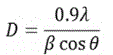
where, λ = 0.154 nm is the X-Ray wavelength, θ is the Bragg angle and β is the line broadening at half the maximum intensity (FWHM) in radians. The d-spacing was calculated by Braggʼs equation λ = 2dsinθ, where d is the interplanar spacing and θ the diffraction angle [21].
The optical study was carried out through transmittance measurements, using a Perkin Elmer Lambda 950 spectrophotometer at a wavelength range of λ = 250-2500 nm. From the transmittance spectrum and the equation T=T0.exp (ad) where T is the measured transmittance, T0 is the glass transmittance (without material), a is the absorption coefficient and d the thickness of the films, the optical energy band gap (Egap) was evaluated by applying a Tauc plot, using the equation:
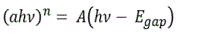
where, α is the absorption coefficient, hv is the photon energy, h is Planckʼs constant and A is a constant. For a direct allowed optical transition, as for ZnO in the present study, n equals 2. From the plot of (ahv)2 vs hv and by linear extrapolation, the energy gap was extracted.
Sensing characterization techniques
The ozone sensing properties of the films were estimated by monitoring electrical and SAW signals respectively at room temperature. Specifically, the conductometric measurements were carried out in a home-made system described else where utilizing a consecutive photoreduction and oxidation process [22]. The photoreduction took place at a vacuum pressure of approximately 10-2 mbar while the samples were directly irradiated by a UV light (mercury pencil lamp with an average intensity of 4 mW/cm2) at a wavelength of 254 nm, placed at a distance of approximately 3 cm from the surface of the film. For the subsequent oxidation process ozone was produced by an ozone analyzer (Thermo Electron Corporation, model 49i) at different concentrations ranging between 5 and 2400 ppb and the chamber was backfilled with ozone at a pressure of 100 mbar. In order to measure the induced electrical changes on the films during the photoreduction-oxidation procedure, a constant voltage was applied during the whole cycling procedure and the electric current was measured by a Keithley 6517A electrometer. In addition, the SAW filter tests took place in a corresponding home-made cell of approximately 30 ml in volume. The cell incorporated a UV pencil style lamp fitting together with a quartz glass located directly opposite the filter structure and it was open to gas flow through inlet and outlet fittings while a labview based program was developed to facilitate automatic computer calculations. ZnO films were deposited onto commercial SAW filters and the whole structure exposed to the same photoreduction and subsequent oxidation processes. The O3 gas concentrations were ranging between 100 ppb and 2 ppm accurately produced by the ozone analyzer. The gas flow rate was kept at 500 standard cm3 / min (sccm) for both processes during all test cycles.
Results and Discussion
Surface, structural and optical properties
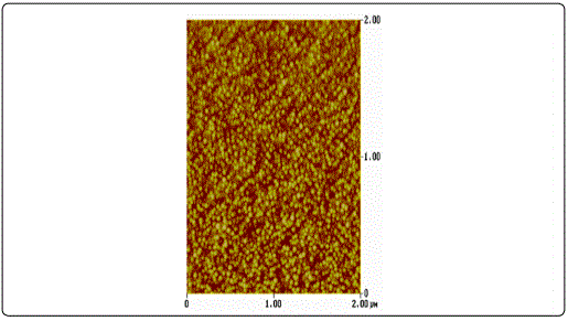
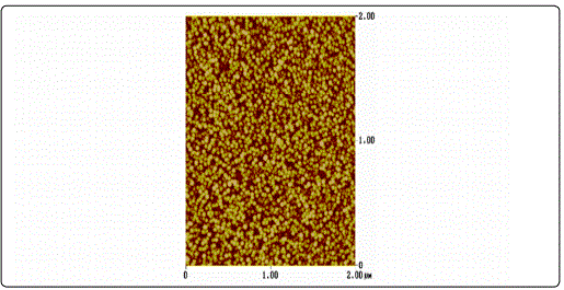
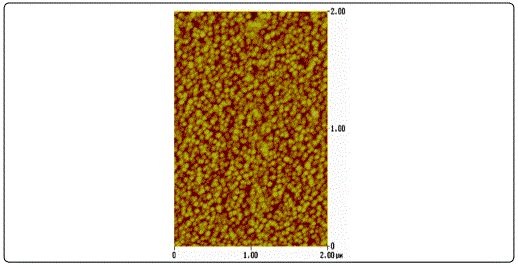
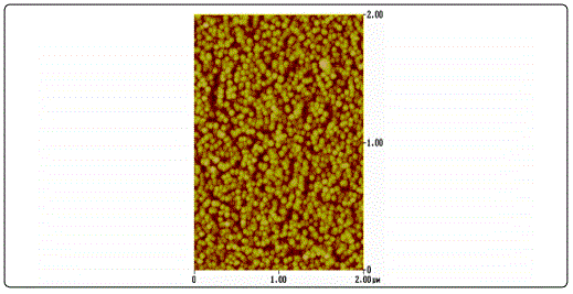
AFM surface characterization of the films showed that all films exhibited granular morphology without any cracks (Figure 1). Furthermore, both the lateral grain size and the RMS roughness were found to increase with film thickness (Table 1), in accordance to the literature [23].
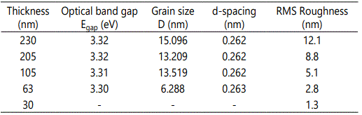

The XRD patterns of the ZnO films shown in Figure 2 were identified as the hexagonal wurtzite zinc oxide, (Joint Committee on Powder Diffraction Standards (JCPDS) card no. 36: 1451) with no impurities. It was apparent that as the thickness increases, the peak intensity at 2θ ≈ 34.4° corresponding to (002) plane increases, whereas its width decreases. This was an indication that the films were growing preferentially along the c-axis orientation, vertical to the substrate, a general observation for sputtered ZnO films [24] [25]. Higher crystallinity was obtained for thicker samples while the film with the thickness of 30 nm been regarded amorphous as diffraction peaks were missing.
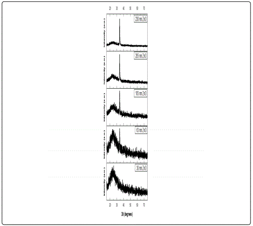
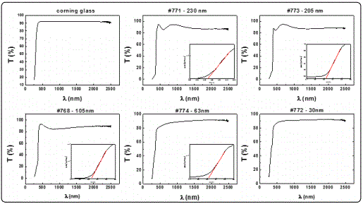
Figure 3 depicts the optical transmittance spectra, T(%), of ZnO films deposited onto Corning glass substrates. It can be seen that all films exhibited a high transparency over 80%, in the visible and NIR regions, which is in line with other studies [24,26]. The optical band gap of ZnO was found to be in the range of 3.32 to 3.30 eV as shown in the insets. The variations of structural and optical characteristics with thickness are being presented in Table 1. It is obvious that both energy band gap and d-spacing remain almost constant, while the grain size increases with thickness, confirming other studies [21,27].
Sensing properties
Conductometric technique
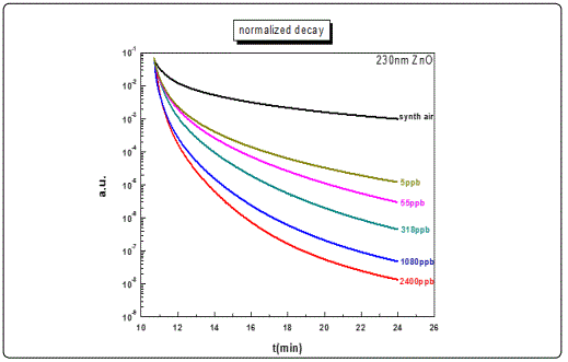
Monitoring of conductivity at different ozone concentration levels provides information on the sensing properties of the films under test. Figure 4 illustrates typical cycles of a consecutive photoreduction-oxidation process for the ZnO film with a thickness of 230 nm. The first oxidation process took place in the presence of synthetic air (20% O2, 80% N2) which was used as the reference signal while the remaining oxidation processes were carried out under different ozone concentrations. The duration of each photoreduction process was 10 min while each oxidation process lasted 15 min.
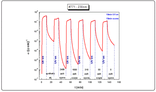
Other films with similar thicknesses exhibited equivalent results (e.g. the 205 nm film). However, for films with lower thicknesses, as in the case of the 105 nm sample (Figure 6, a) and less, although the response rate was satisfactory (3 orders of magnitude), the decay curves to different ozone levels concentrations could not be adequately distinguished, exhibiting poor resolution (Figure 6, b). This behaviour was attributed to the specific growth conditions and the corresponding film crystalline structure, and maybe associated with the depleted area created following the photoreduction cycles.
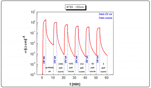
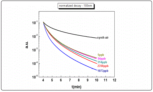
It is widely accepted that for the metal oxide gas sensing elements, during the photoreduction process, oxygen bonds are breaking leading to the creation of oxygen vacancies in a process by which two electrons are being released for each missing oxygen [31]. In the subsequent process of oxidation, the sensitivity of the sensing elements seems to be subject to the presence of the oxidizing gas (O3) i.e. decreases with the decrease of ozone concentration levels while the response is higher at higher concentration levels [28,29]. The recorded gradual drop in the observed maximum conductivity levels after the photoreduction process, particularly for the thinner films may be attributed to the fact that the oxygen vacancies in the photoreduced film are not fully occupied by the oxygen atoms of the ozone molecules during the oxidation process. Therefore by decreasing the ozone concentration level the response obtained, after the photoreduction, was lower. For the thinner samples in particular, the developed oxygen vacancies during photoreduction may initially be occupied completely from the first ozone concentration levels during the oxidation process thus leading to a fast saturation. Such a process already observed in the past, seems to be reproducible and consistent with each and every photoreduction-oxidation test cycle [8].
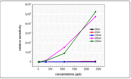
The sensitivity of films with different thickness was calculated as the ratio of the maximum to minimum conductivity values, (S=σmax/σmin) [1] and their normalized relative sensitivity responses as a function of ozone concentration levels are presented in Figure 7. It is apparent that for ozone concentrations below 500 ppb the sensitivity of almost all sputtered films remains constant and any variations are within one order of magnitude only, independent of the film thickness. This denotes the films inability to safely distinguish among O3 concentrations in this low volume range. On the other hand, for ozone concentrations above 500 ppb and thickness above 200 nm the responses are obviously much larger, implying that although the ZnO sensing materials can detect ultra low ozone levels of the order of a few ppb, they lack the required resolution at concentrations below 500 ppb, exhibiting a much better ability to distinguish between higher ozone levels. Comparing the present results with those existing in the literature, it is confirmed that the conductivity and gas sensitivity increase with the increase of the crystallite size [32], and consequently with the increase of the thickness.
SAW technique
Contrasting the above results with the SAW technique, two major interactions i.e. the mass loading and acousto-electric effects were studied utilizing commercially available SAW filters. The first effect is associated with a noticeable frequency shift originating from mass loading. In particular, due to the deposition of a thin ZnO film, used as the sensitive layer, on top of the SAW filter, a small shift towards lower frequencies is being recorded, however, with no noticeable changes to the filter attenuation signal [33]. This happens, because any increase in the kinetic energy density (due to the wave movement on the surface) results in a decrease in the wave velocity, hence in the signal transmission frequency (v = u / λ, where v: frequency, λ: wavelength and u: velocity). Following this initial frequency shift which should remain constant (its value is considered as the central reference frequency for detecting subsequent acoustic wave velocity variations) any surface perturbations as a result of a photoreduction and oxidation processes on the sensing film surface are recorded with distinct clarity.
In order to examine the acousto-electric behavior of the SAW filters utilizing a thin sensing film of ZnO (ZnO/SAW) on top, and the resulting frequency shifts as a response to surface perturbations, filters with a nominal central operating frequency of 930 MHz were selected. Their responses as a function of different ZnO thicknesses were tested towards ozone with varying concentrations at room temperature conditions. Figure 8, a-c depicts typical centre frequency variations towards consecutive photoreduction-oxidation cycles against four different ozone concentrations. Every cycle lasted 15 min, of which 5 min were dedicated for the photoreduction process while 10 min was the duration of each oxidation process. The studied film thicknesses of the ZnO films were limited to less than 100 nm as any greater thickness imposed a significant mass loading effect, therefore additional stress which subsequently introduced an operating malfunction on the sensitivity of the selected SAW filters resulting in significant deviations from their normal operational characteristics.
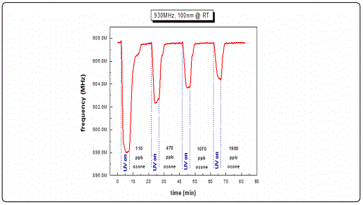
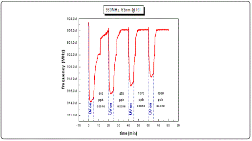
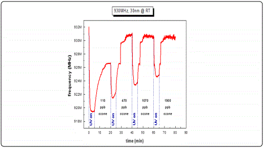
Results from ZnO films with thicknesses less than 100 nm revealed a decrease in the filterʼs centre frequency under UV illumination and a subsequent frequency increase under ozone exposure during a photoreduction-oxidation cycle. This behavior is in good agreement with published works [27,32,34] where other oxidizing gases such as NO2 were used. Analysing the present results in more detail, we observed frequency response of the order of 8-9 MHz in the commercial SAW filters following the deposition of the ZnO sensitive layer with thickness ranging between 30-100 nm. This was due to the mass loading effect and is justified by the fact that the sensing material (ZnO) is highly insulating i.e. induces no inherent acousto-electric effects. In a study presented by B. Raj and co-workers in 2013 [35] ZnO/SAW deposited by sputtering was compared with other metal oxides (SnO2, TeO2 and TiO2) and they found that ZnO, in a parametric study on the thickness dependence, exhibited higher responses under a selected reducing gas (ammonia) exposure. These results are in a good agreement with the present work during which we achieved to obtain detectable responses towards ultra-lower O3 concentrations at a range of low film thickness. Alternative studies on ZnO nanoparticles deposited by spin coating onto SAW devices by Phan and co-workers in 2012 [36] on hydrogen sensing applications concluded that a layered SAW structure may exhibit a frequency shift at low H2 concentration at room temperature with good repeatability and stability. However in this study the maximum measured shift was in the order of kHz. As opposed to our results obtained at RT, their good response was due to the postannealing process and consequently improvement of the films crystallinity properties. In the present study, following subsequent analysis applying cycles of photoreduction and oxidation, a noticeable drift of the base line frequency was recorded, denoting an increasing memory effect during the initial stages of the oxidation state particularly for the lower thickness films and at low O3 concentrations. It is apparent that as the gas concentration increases the recorded frequency response increases. This may be attributed to the fact that as ozone is induced into the test chamber, an increased coverage of the vacancies sites is induced, resulting to an excess of oxygen presence on the surface sites. Figure 9 depicts a complete single photoreduction-oxidation cycle of the film with thickness 30 nm which is subjected to a more detailed subsequent analysis hereby. When the photoreduction process starts with UV light on, the process competes with an inherent oxidation process due to the O3 formation by the UV radiation on the poor vacuum environment (10-2 mbar) of the test chamber. (Figure 9, region A1) the analysis of the obtained results, it is observed that after several seconds and while the samples are still illuminated by the UV lamp, a frequency increase takes place which is attributed to the fact that exposure of the film to the UV light in an environment that there are oxygen molecules, the photoreduction is losing to an oxidation process that takes place while the films is under UV illumination [37] (Figure 9, region A2). Further analysis revealed that in the absence of UV light and simultaneous ozone introduction into the test chamber, the main oxidation process initiates. During this stage, a two-step procedure seems to be involved, one attributed purely to an electric current variation (reduction) due to the capture of free electrons created during the UV photoreduction process and another, most probably associated with mechanical induced changes possibly attributed to the piezoelectric substrate material. This effect was more intense on filters with thin sensing layers.
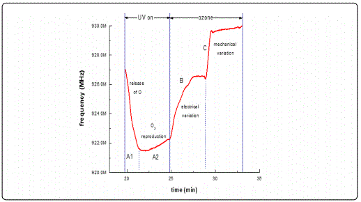
In more detail, the region marked as B in Figure 9 represents the first step of the oxidation process and can be attributed to the SAW acousto-electric effect. This sensing behaviour corresponds exactly to the earlier results from the conductometric response already analysed and are attributed to surface phenomena. It must be emphasized, that this step ends at the same frequency value and is dependent of the gas concentration, indicating that it is a purely surface transport phenomenon as confirmed by conductometric measurements. The second step of the oxidation process, marked as C (Figure 9), is probably related to a mechanical phenomenon relevant to the nature of the SAW transducer used as substrate material rather than a direct acousto-electric effect. Supporting evidence on this argument is the fact that no such behaviour has ever been reporting on metal oxide sensing layers deposited on other rigid or flexible substrates. Therefore, it is believed that this is most likely a phenomenon concerning the mechanical properties of the used substrate i.e. it is directly related to the elasticity of the piezoelectric substrate. Such a change in a SAW filter mechanical properties may be attributed to the interaction of ozone with the SAW structure itself that leads to changes to its elastic (Youngʼs) modulus. In general piezoelectric materials couple electrical and mechanical effects along with thermal effects therefore they are sensitive to a number of parameters. These are usually described by the following relations [19]:
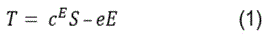
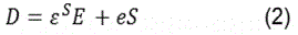
in which T is the mechanical stress (Nm-2), S is the stiffness with constant electric field, S is the mechanical strain, e is the piezoelectric stress constant (Cm-2), E is the electric field (Vm-1), D is the electric displacement (Cm-2), and ε is the permittivity (CV-1m-1) at constant strain [19]. From the above relations and experimental data it becomes apparent that the introduction of ozone causes electrical variations (represented in B region) which are leading to a decrease in conductivity; this is something also confirmed by the above conductometric results (Figure 4 & Figure 6a). While still under O3 exposure (region B) the free electron capture process is getting saturated (plateau at the end of region B) and any electrical variations are terminated leading to a constant electric field presence. If this is true, the second term in the right-hand side of Eq.1 remains constant denoting a relation between stress and strain (Youngʼs modulus). Therefore, ozone introduction may result to mechanical variations through elasticity changes of the SAW filter substrate material which in turn induce additional stress (T). These variations may then lead to an increase in the acoustic wave velocity and hence the propagating frequency (see region marked as C) which is also confirmed by similar reports published by others [35,38].
In conclusion it is suggested that these frequency changes may be attributed to induced mechanical variations of the SAW filter posed by the presence of ozone atmosphere, a result which requires further verification through additional future work.
Summarizing the results of the present work, one may conclude that ZnO films grown by DC sputtering are very promising candidates for ozone sensing applications capable to detect concentrations of the order of a few ppb at room temperature. Although, the use of SAW filters induces additional implications on the signal responses which combined with the fact that there is no recorded improvement in the ozone detection limits compared to the single conductometric technique renders the SAW, as a technique itself, applicable only in dedicated applications for which integration of a SAW filter may be regarded more advantageous than a simple conductometric set-up.
Conclusion
The ozone sensing properties of zinc oxide utilizing a conductometric set-up as bench-mark for surface acoustic wave gas sensors were studied. All films, with the exception of the 30 nm thick film were polycrystalline as revealed from the XRD analysis, with the preferential orientation along the c-axis in the (002) plane. They also exhibited a high transparency (> 80%) in the visible region. AFM images of their surfaces revealed that roughness increases along with thickness. Sputtered films with different thicknesses have showed conductivity changes of up to 5 orders of magnitude during a photoreduction-oxidation cycle. As far as SAW results are concerned, the study has shown that, due to the mass loading effect, a decrease of the centre frequency takes place along with the deposited ZnO sensitive layer. The acousto-electric response appeared to be the dominant effect regarding electrical conductivity variations. The acousto-electric effect revealed a good response of the sensing element with a frequency shift of a few MHz. SAW filter sensing analysis revealed that the oxidation process is mainly a two-step procedure. The first step was attributed solely to the induced electrical variation while the second to the mechanical variations, possibly originating from the substrate piezoelectric properties. Comparing the conductometric with the SAW technique one may conclude that the first technique is preferable for an accurate account of ultra-low O3 concentrations.
Acknowledgments
The support through the FP7-Regpot-2012-2013-1 project under grant agreement No 316165 is highly appreciated.
References
- Bender M, Fortunato EP, Nunes A, et al. Highly sensitive ZnO ozone detectors at room temperature. Japanese J Appl Physics, Part 2 Lett. 2003; 42(4 B): 2-5. doi: 10.1143/JJAP.42.L435
- Look DC. Recent advances in ZnO materials and devices. Mater Sci Eng B Solid-State Mater Adv Technol. 2001; 80(1-3): 383-87. doi: 10.1016/S0921-5107(00)00604-8
- Suchea M, Christoulakis S, Moschovis K, Katsarakis N, Kiriakidis G. ZnO transparent thin films for gas sensor applications. Thin Solid Films. 2006; 515(2): 551-54. doi: 10.1016/j.tsf.2005.12.295
- Kortidis I, Moschovis K, Mahmoud FA, Kiriakidis G. Structural analysis of aerosol spray pyrolysis ZnO films exhibiting ultra low ozone detection limits at room temperature. Thin Solid Films. 2009; 518(4): 1208-13. doi: 10.1016/j.tsf.2009.08.018
- Lee GH, Kawazoe T, Ohtsu M. Difference in optical bandgap between zinc-blende and wurtzite ZnO structure formed on sapphire (0001) substrate. Solid State Commun. 2002; 124(5): 163-65. doi: 10.1016/S0038-1098(02)00537-9
- Martinez-Perez L, Munoz-Aguirre N, Munoz-Aguirre S, Zelaya-Angel O. Nanometric structures of highly oriented zinc blende ZnO thin films. Mater Lett. 2015; 139: 63-65. doi: 10.1016/j.matlet.2014.10.054
- Özgür Ü, Alivov YI, Liu CA, et al. A comprehensive review of ZnO materials and devices. J Appl Phys. 2005; 98(4): 1-103. doi: 10.1063/1.1992666
- Bender M, Gagaoudakis E, Douloufakis E, et al. Production and characterization of zinc oxide thin films for room temperature ozone sensing. Thin Solid Films. 2002; 418(1): 45-50. doi: 10.1016/S0040-6090(02)00588-6
- Ippolito SJ, Kandasamy S, Kalantar-Zadeh K, et al. Highly Sensitive Layered ZnO/LiNbO3 SAW Device with InOx Selective Layer for NO2 and H2 Gas Sensing. Sensors and Actuators B: Chemical. 2005; 111–112: 207-12. doi: 10.1016/j.aca.2012.05.048
- Özgür Ü, Hofstetter D, Morkoç H. ZnO Devices and Applications: A Review of Current Status and Future Prospects. Proc IEEE. 2010; 98(7): 1255-68. doi: 10.1109/JPROC.2010.2044550
- EPA. NAAQS Table | Criteria Air Pollutants. https://www.epa.gov/criteriaair-pollutants/naaqs-table. Published 2008.
- Atashbar MZ, Gong B, Sun HT, Wlodarski W, Lamb R. Investigation on ozone-sensitive In2O3 thin films. Thin Solid Films. 1999; 354(1): 222-26. doi: 10.1016/S0040-6090(99)00405-8
- Thirumalairajan S, Mastelaro VR. A novel organic pollutants gas sensing material p-type CuAlO2 microsphere constituted of nanoparticles for environmental remediation. Sensors Actuators, B Chem. 2016; 223: 138-48. doi: 10.1016/j.snb.2015.09.092
- Wu CH, Jiang GJ, Chang KW, Lin CW, Chen KL. Highly sensitive amorphous In-Ga-Zn-O films for ppb-level ozone sensing: Effects of deposition temperature. Sensors Actuators, B Chem. 2015; 211: 354-58. doi: 10.1016/j.snb.2015.01.048
- Kang BS, Heo YW, Tien LC, et al. Hydrogen and ozone gas sensing using multiple ZnO nanorods. Appl Phys A. 2004; 80(5): 1029-32. doi: 10.1007/s00339-004-3098-8
- Hoummady M, Campitelli A, Wlodarski W. Acoustic wave sensors: design, sensing mechanisms and applications. Smart Mater Struct. 1997; 6(6): 647-57. doi: 10.1088/0964-1726/6/6/001
- Papadaki D, Foteinis S, Mhlongo GH, et al. Life cycle assessment of facile microwave-assisted zinc oxide (ZnO) nanostructures. Sci Total Environ. 2017; 586: 565-75. doi: 10.1016/j.scitotenv.2017.02.019
- Lin S, Huang J, Lii D. Effect of substrate temperature on the properties of Ti-doped ZnO films by simultaneous rf and dc magnetron sputtering. Mater Chem Phys. 2005; 90: 22-30. doi: 10.1016/j.matchemphys.2004.08.040
- Ahmadipour M, Ain MF, Ahmad ZA. Effect of thickness on surface morphology, optical and humidity sensing properties of RF magnetron sputtered CCTO thin films. Appl Surf Sci. 2016; 385: 182-90. doi: 10.1016/j.apsusc.2016.05.098
- Bedia A, Bedia FZ, Aillerie M, et al. Optical, electrical and structural properties of nano-pyramidal ZnO films grown on glass substrate by spray pyrolysis technique. Opt Mater (Amst). 2014; 36(7): 1123-30. doi: 10.1016/j.optmat.2014.02.012
- Tseng JY, Chen YT, Lin CJ, et al. The optical, electrical, and nanomechanical properties of ZnO thin films. Opt - Int J Light Electron Opt. 2015; 126(21): 3263-66. doi: 10.1016/j.ijleo.2015.07.126
- Musat V, Rego AM, Monteiro R, Fortunato E. Microstructure and gassensing properties of sol-gel ZnO thin films. Thin Solid Films. 2008; 516(7): 1512-15. doi: 10.1016/j.tsf.2007.07.198
- Kiriakidis G, Moschovis K, Kortidis I, Binas V. Ultra-low gas sensing utilizing metal oxide thin films. Vacuum. 2012; 86(5): 495-506. doi: 10.1016/j.vacuum.2011.10.013
- Cheng XL, Zhao H, Huo LH, Gao S, Zhao JG. ZnO nanoparticulate thin film: Preparation, characterization and gas-sensing property. Sensors Actuators, B Chem. 2004; 102(2): 248-52. doi: 10.1016/j.snb.2004.04.080
- Shao C, Chang Y, Long Y. High performance of nanostructured ZnO film gas sensor at room temperature. Sensors Actuators, B Chem. 2014; 204: 666-72. doi: 10.1016/j.snb.2014.08.003
- Huang J, Wu Y, Gu C, Zhai M, Sun Y, Liu J. Fabrication and gas-sensing properties of hierarchically porous ZnO architectures. Sensors Actuators, B Chem. 2011; 155(1): 126-33. doi: 10.1016/j.snb.2010.11.036
- de Lacy Costello BPJ, Ewen RJ, Ratcliffe NM, Richards M. Highly sensitive room temperature sensors based on the UV-LED activation of zinc oxide nanoparticles. Sensors Actuators, B Chem. 2008; 134(2): 945-52. doi: 10.1016/j.snb.2008.06.055
- Ippolito SJ, Kandasamy S, Kalantar-Zadeh K, et al. Highly sensitive layered ZnO/LiNbO3 SAW device with InO x selective layer for NO2 and H2 gas sensing. Sensors Actuators, B Chem. 2005; 111-112(SUPPL.): 207-12. doi: 10.1016/j.snb.2005.07.046
- Cheeke JDN, Wang Z. Acoustic wave gas sensors. Sensors Actuators B Chem. 1999; 59(2-3): 146-53. doi: 10.1016/S0925-4005(99)00212-9
- Matatagui D, Fernandez MJ, Fontecha JL, et al. Propagation of acoustic waves in metal oxide nanoparticle layers with catalytic metals for selective gas detection. Sensors Actuators B Chem. 2015; 217: 65-71. doi: 10.1016/j.snb.2014.12.076
- Bhasker Raj V, Singh H, Nimal AT, Tomar M, Sharma MU, Gupta V. Effect of metal oxide sensing layers on the distinct detection of ammonia using surface acoustic wave (SAW) sensors. Sensors Actuators, B Chem. 2013; 187: 563-73. doi: 10.1016/j.snb.2013.04.063
- Phan DT, Chung GS. Surface acoustic wave hydrogen sensors based on ZnO nanoparticles incorporated with a Pt catalyst. Sensors Actuators B Chem. 2012; 161(1): 341-48. doi: 10.1016/j.snb.2011.10.042
- Martins R, Fortunato E, Nunes P, et al. Zinc oxide as an ozone sensor. J Appl Phys. 2004; 96(3): 1398-108. doi: 10.1063/1.1765864
- Jakubik WP. Surface acoustic wave-based gas sensors. Thin Solid Films. 2011; 520(3): 986-93. doi: 10.1016/j.tsf.2011.04.174
