

Review Article
Fabrication and Superconducting Property study of 1D Single Crystalline Metal Nanowires
1State Key Laboratory for Heavy Oil Processing, PetroChina Key Laboratory of Catalysis, China University of Petroleum, China
2Departmentof Chemical and Biomolecular Engineering, Hong Kong University of Science and Technology, Clear Water Bay, Kowloon, Hong Kong
*Corresponding author: Xijun Hu, Professor, Department of Chemical and Biomolecular Engineering, Hong Kong University of Science and Technology, Clear Water Bay, Kowloon, Hong Kong. E-mail: kexhu@ust.hk
Received: October 3, 2016 Accepted: November 3, 2016 Published: November 8, 2016
Citation: Zhang Y, Hu X, Yan Z. Fabrication and Superconducting Property study of 1D Single Crystalline Metal Nanowires. Madridge J Nanotechnol Nanosci. 2016; 1(1): 29-43. doi: 10.18689/mjnn-1000108
Copyright: © 2016 The Author(s). This work is licensed under a Creative Commons Attribution 4.0 International License, which permits unrestricted use, distribution, and reproduction in any medium, provided the original work is properly cited.
Abstract
Physical properties of quasi-one-dimensional superconducting nanowires can differ significantly from those of bulk superconductors. The reason behind is the impact of thermal and quantum fluctuations. In the particular case of resistive measurements, the fluctuations may significantly broaden the superconducting transition R(T). For superconducting wires with diameters decreasing, quantum phase slippage is an important process which can yield a non-vanishing wire resistance down to very low temperatures. Further decrease of the wire diameter results in proliferation of quantum phase slips causing a sharp crossover from superconducting to normal behaviour. The critical magnetic field exhibits quantum-size oscillations with pronounced resonant enhancements as a function of the wire radius. The understanding of the nature of superconductivity is often limited by the sampleʼs morphology (e.g., disorder, defects, grain boundaries, or crystallinity). In order to identify the intrinsic phenomena in 1D, experimental studies of single crystal nanowires are clearly desirable. In this review, we present a summary of some recent activities in the field with main emphasis on experiment, while brief theoretical background is also presented.
Keywords: Fabrication; Superconducting nanowires; Magnetic field; Crystallinity.
Introduction
Advances in fabrication now allow the production of high-quality wires whose diameters are smaller than the superconducting coherence length. In this regime, transverse excitations in the superconducting order parameter are energetically less favourable, and the system approaches the 1D limit where the role of thermal fluctuations is more important than in 3D. Thus, superconductivity in quasi-one-dimensional (quasi-1D) nanowires is one of the most intriguing problems in condensed-matter physics [1-6]. Many interesting physical phenomena, such as thermally activated phase slip [7-9], quantum phase slip [10-11], superconductor-insulator transition [12] and proximity effect [13-14], were observed in quasi-1D systems [15-16] Magnetic field lifts the time reversal symmetry of the spin and orbital states of paired electrons and suppresses the superconducting transition [17]; many interesting results such as magnetoresistance oscillations were also observed under a magnetic field [18-20]. Since the most detailed work in 1D or two-dimensional superconducting systems has been carried out in polycrystalline or amorphous samples, our understanding of the nature of superconductivity is often limited by the sampleʼs morphology (e.g., disorder, defects, grain boundaries, orcrystallinity). In order to identify the intrinsic phenomena in1D, performing experiments on a system having the least possible variations in morphology and microstructure could not only clarify the mechanisms of phenomena but also allow the exploration of new properties. Therefore, to understand these interesting behaviours, singlecrystal superconducting systems with controlled dimensionality are highly desirable. Yi et al [21] found the transition temperature in single crystal wires is close to thebulk TC, but significantly suppressed in polycrystalline wires. Michotte et al [22] found superconductivity of Pb nanowires survives only in thicker polycrystalline wires (i.e., for diameters .50 nm) with single-crystal segments, and resistance of wires of diameter below 50 nm increase with decreasing temperature below 10 K, with no evidence of superconductivity due to “poor crystal structure”. Tian et al. [23] found much more PSCs along the length in single crystal Sn wires than the polycrystalline wire might be due to single crystalline and polycrystalline morphology. These experiments further confirm the need of measurement on quasi-1D single-crystal wires. Here we present an overview of recent results on superconducting nanowires in the quantum-size regime with main emphasis on experiment, while brief theoretical background is also presented.
Superconducting metal nanowires Nb nanowires
Since Nb is the most studied among the superconducting elements due to its high Tc (9.5 K) and the most used in superconducting electronics, it represents the most suitable material to test new possible applications of the superconductivity at the nanoscale.
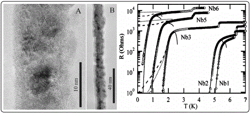
Continuous Nb wires, 7–15 nm in diameter, have been fabricated by sputter-coating single fluorinated carbon nanotubes by Rogachev et al [24]. The resistance versus temperature, R (T), as shown in Figure 1 (c) were well described by the Langer–Ambegaokar–McCumber–Halperin (LAMH) theory of thermally activated phase slips. Quantum phase slips were not observed. This possibly because the thicker polycrystalline Nb wires deposited on carbon nanotubes do not have weak links, and the grain boundaries seen in the TEM image (Figure 1a) do not produce tunneling barriers for supercurrent. It is quite surprising that the in homogeneities in granular Nb nanowires do not seem to broaden the R (T) curves, which can be fitted by the TAPS model developed forhomogeneous quasi-1D systems.
a=51 and B=51. The dotted lines are computed with a=51.3 and B=57.2.
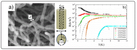
Nb layers with dNb in the range 3-50 nm were deposited on CNT films by high-vacuum dc magnetron sputtering with a starting pressure in the low 10-8 mbar regime and in an Ar+ deposition pressure of 4mbar[25]. The main panel of Figure 2(a) showed a scanning electron microscope (SEM) micrograph of CNTNb3. As sketched in the inset, the dot-ended line in the figure gives d dCNT +2dNb, where dCNT =9.5 nm and, for this sample, dNb=3 nm. In Figure2 (b), decreasing dNb, Tcon remained finite, while full superconducting behavior was inhibited down to the lowest measured temperature (T=250 mK) as observed for the samples CNTNb30 and CNTNb20. The sample with the thinnest Nb layer, CNTNb10, presented a semiconducting behavior without any trace of superconductivity. This suggested the presence of a superconductor-insulator (S-I) transition with decreasing dNb with RNRQ (RN was the normal state resistance measured just before of the superconducting transition, RQ was the quantum resistance)as a crossover resistance. This result, observed in many low dimensional materials [26] as well as in SNWs [27,28], found many controversial explanations [26]. In the case of SNWs it is interpreted in terms of charge localization [27], or as due to local magnetic moments pres ent in the wire [29]. Other mechanisms such as, for example, electron interactions with surface photons [30], invoked as possible cause of the reduction of Tc [31] and of the S-I transition [26] in low dimensional systems. In fact, being the Tcon of the aggregates of SNWs and of the reference films the same, the electron-phonon (eph) coupling constant in these systems should also be the same. Therefore, the S-I transition should be ascribed to other causes. A more intriguing explanation concerns the nature of weak link constrictions (WLCs) presented inside a single polycrystalline SNW at the interfaces between the grains. In this case, the insulating or metallic nature of the WLCs determines if RN > RQ or RN< RQ [25]. The hypothesis of the WLC at the base of the appearance of the S-I transition seems to be the most appropriate due to the large number of interfaces present in CNTNb systems. In fact, for low values of dNb, the weak coupling between the interfaces WAS favored with the consequent development of the S-I transition.
Ultrathin nanowires of niobium, with diameters of 4.2 nm and perfectly clean surface, were grown in quantized vortices of superfluid helium [32]. The superconducting transition in the thin niobium nanowire was found to be distorted and strongly shifted towards lower temperatures. Superconducting niobium wires allowed a high rate of quantum phase slip. This phase slippage led to a phase transition to an insulating state at T→0 (shown in Figure 3(c)). This was in agreement with thetheory of quantum phase slips advanced by Z aikin and co-workers [33] which predicts an insulating state at T = 0. In this theory a superconducting to insulator transition critical point was expected to be controlled by the diameter of the nanowire. The critical diameter was estimated to be a few nanometers. The resistance is predicted to diverge in the insulating phase according to a power low, RT.
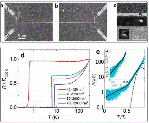
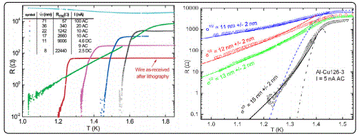
The Nb nanowires of 6 mm long with different cross-sectional dimensions (shown in Figure 4a,b) were fabricated using standard e-beam lithography processes [34]. A low-temperature residual resistance tail measured with an excitation current of 5 nA was found in the thinnest wire down to 50 mK or 7.7% of Tc of Nb (shown Figure 4d, e). The functional form of the residual resistance was consistent with quantum phase slip (QPS) processes and was well described by eq 1 as proposed by Giordano [11]. According to eq 1, authors defined y=r/(1-T/Tc)3/4and x=1-, a plot of log(y) versus x in the low temperature regime should be a straight line if the measured resistance is dominated by QPS. The inset of Figure 4e confirmed this expectation. Moreover, resistance measured at high bias excitation current switched among many discrete values that were well below the normal state resistance. These discrete resistance values as a function of temperature falled into several parallel curves (shown Figure 5) all showing QPS-like decay in the low temperature limit similar to that found at low current. This phenomenon was not observed in the previous QPS experiments in micron long nanowires with either low or high currents and constitutes the key new result of Zhaoʼs work. They quantified the length of the phase slip centers, which at about 40 μm was longer than the nanowires used in prior phase slip experiments but much shorter than their NbNW. The latter condition leaded to a situation that sections of the wire near phase slip centers turned normal while regions far from the phase slip centers stayed in superconducting phase and exhibited QPS-like temperature dependence in the low temperature limit similar to that found with low excitation current.
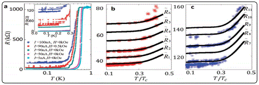
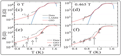
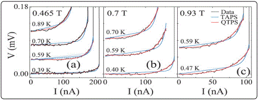
Xu et al [35] reported a general method, superlattice nanowire pattern transfer (SNAP), for reliably fabricating quasi-one-dimensional superconducting nanowire arrays, with good control over nanowire cross section and length, and with full compatibility with device processing methods. The ability to fabricate very long (up to 100 μm) NWs with different lengths but identical cross sections has for the first time allowed for the investigation of lengthʼs sole influence on superconductivity in NWs, which are truly quasi1D superconductors at any temperature. Nearly atomically straight Nb nanowires with widths ranging from bulklike to 10 nm and aspect ratios approaching 104 were prepared. Superconductivity was observed on all Nb nanowires arrays (Figure 6a). The superconductivity was partially suppressed (Tc ~3.5 K as compared with Tc ~5 K for Nb contactedNWs of similar dimensions). The shorter NW array had a lower Tc due to higher suppression from the contacts. The thinner NWs had a lower Tc, with the cross-section dependence of Tc in general agreement with data on CNT-templated NWs [36]. Thinner Nb NW arrays (11 nm × 16 nm × 20μm) was fitted well to TAPS and QPS theories in the low-T limit, as shown in Figure 6b. The similar but shorter NWs deviated from QPS prediction. Such behaviour has been reported in short NWs [36-40], whereas long NWs typically show the expected QPS behaviour [41-43]. The authors concluded that QPS can be partially suppressed in short NWs in the low-T limit due to contact effects. Qualitatively different behaviours were also found for NWs with the same cross section but different lengths in Figure 6d and e. In comparison with a single jump between the superconducting and normal states at Ic for shorter NWs (Figure 6d), longer NWs first enter an intermediate state at Ic, and jump to the normal state at a higher current level, IN ~ 2Ic (Figure 6e). This intermediate region exhibited multiple voltage jumps (Figure 6e inset). Such behaviour was characteristic of long quasi-1D superconductors, and each voltage jump was associated with the emergence of a localized resistive “phase-slip center” (PSC) along the wire. In contrast to the stochastic TAPS and QPS events, PSCs are stable and have fixed locations for a constant driving current. Each PSC occupies a characteristic length of ~2ɅQ*, where ɅQ*~10μm is the quasiparticle diffusion length. The number of PSCs a wire can accommodate should be ~L/2 ɅQ*. But the results on NWs, which were truly quasi1D superconductors at any temperature, have been limited. For example, in electrodeposited Sn NW arrays, PSCs were pinned down at local defects, and the number of PSCs observed was independent of the length of the arrays [23].
Pb nanowires
Bulk Pb is a well-known elementary superconductor with 83 nm coherence length. Therefore, Pb nanowires thinner than ~80 nm are potential candidates to study the complex quasi-1D superconducting transition and associated finite size effects. Low dimensional Pb nanostructures have been ext ensively studied for decades [19, 44-49]. Additionally, amorphous and granular nanowires of Pb and other materials ha ve been studied systematically [1, 15, 19]. In the last few years, there are a number of experiments studying the properties of single crystal superconducting nanowires with diameter less than 100nm [23]. An overarching theme of these studies is to understand how superconductivity in these wires goes away with decreasing diameter.
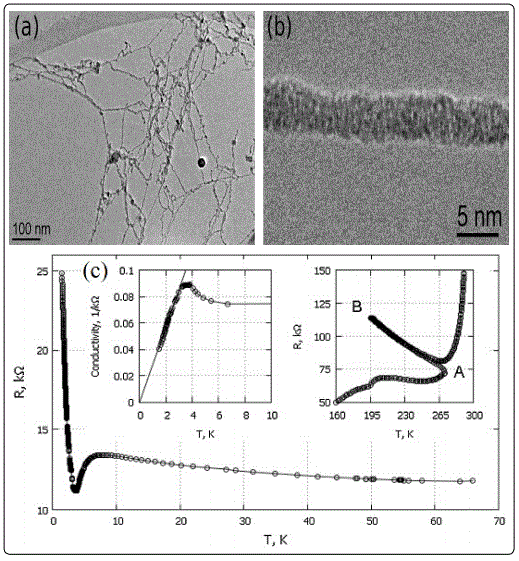
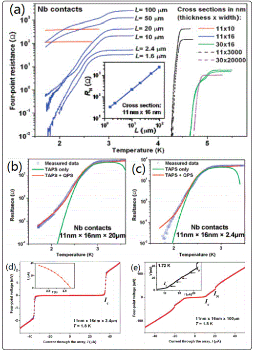
Lead nanowires with high aspect ratio and diameter from 40 to 270 nm have been grown by electrodeposition inside nanoporous polycarbonate membranes [50]. The thinner Pb nanowires were found to be polycrystal with good quality single-crystal regions extending over several microns(asshown in Figure7a and b), and Figure 7c and d revealed the Pb nanowires with 95 nm in diameter appear to have a monocrystalline fcc structure. For small nanowires diamet er (56 nm), Ginzburg–Landau theory [51] allowed one to deduce that vortices did not penetrate nanowires. In contrast, for large nanowire diameter (270 nm), it was shown that one vortex likely penetrated the nanowires at low temperature.
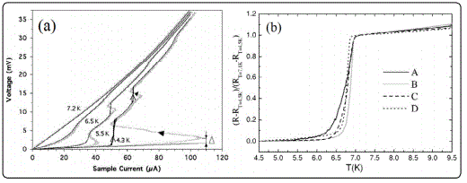
Michotte et al[52], [22] reported transport properties of single lead granular nanowires grown by an electrodeposition technique with uniform diameter of ~40 nm and a very large aspect ratio (~500). Due to the granular character of the nanowire, phase fluctuations were dominant and gave a non-zeroresistance presenting different stages in the superconducting state which caused by the formation of phase slip centers. Moreover, DC voltage driven measurements revealed the existence of a new S-shape behavior near the formation of these phase slip centers, as shown in Figure 8. A theoretical analysis based on the generalized TDGL equations [53] gives a qualitative explanation of this phenomenon which is driven by a highly nonlinear time response of the superconductor to electric fields leading to the periodic creation of PS centers. Experiments with individual Pb nanowires showed clear superconducting transitions, which got broadened with reduction of the sample diameter (Figure 8b [54]. Unfortunately no theory fits was provided by the authors, while the linear scale of the reported R (T) dependencies complicates an independent quantitative comparison.
Another set of quench condensed granular Pb nanowires with cross-section areaσ down to 15 nm2 and length L ranging from 1 to 2 μm was performed by Dynes and co-workers [12]. The samples edge roughness was claimed to be about 3 nm. A remarkable feature of the method is the ability to vary the wire thickness and, hence, its cross-section at a constant width w in situ inside the cryostat in between the sessions of truly 4-probe R(T) measurements. The experiments clearly indicated systematic deviations of the experimental data points R(T) from the TAPS model predictions. This discrepancy increases as the wires become narrower. The width of the superconducting transition was found to scale with thenormal state resistance RN . It should be noted that in lead nanowires as narrow as 15 nm and as thin as 10 nm no low temperature resistance tails were observed. Instead, a less dramatic but systematic broadening of the superconducting transition beyond the TAPS limit was noted.
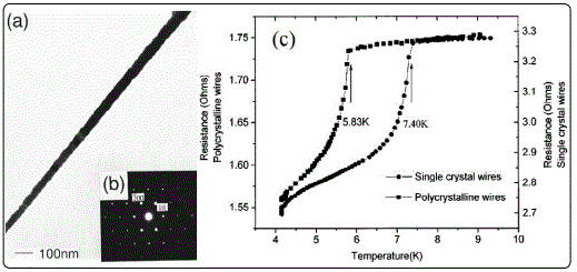
Single crystal superconducting Pb wires (diameter~50 nm) (Figure 9a) prepared by pulse electrode position innanoporous membranes [21] showed significantly higher superconducting transition temperature Tc than that of polycrystalline ones (Figure 9b). The author attributed this to the possible reasons:
(i) homogeneous disorder, which was reasonable, given that the grain boundary separation in the polycrystalline Pb nanowires wass less than the coherence lengthξ0 for (Pb ~83 nm);
(ii) The thermal conductivity of the polycrystalline nanowires was so low compared to that of the single-crystal ones that their Tc appears suppressed.
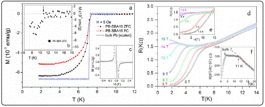
He et al [55] fabricated ultrathin lead (Pb) nanowires in the 6 nm pores of SBA-15 mesoporous silica substrates by chemical vapor deposition.The quasi-1D nature of the material causes obviously a more continuous transition in contrast to the sudden occurrence of the Meissner effect in bulk Pb, as shown in Figure 10a. shows an enlarged transition onset. A tiny but sharp downturn in the ZFC magnetization at 11 K resolved in Figure 10b suggested that the nanostructure induces weak diamagnetic fluctuations, 3~4 K above the bulk Tc. Tc enhancements in nanomaterial have been previously observed [56-59], but in this ultrathin Pb nanowires the effect was particularly strong. The surface of the thin nanowires represents a significant fracti on of the total volume, and phonon softening [60] can cause a locally higher Tc. As seen in Figure 10d, magnetic fields suppress the transition until the normal state was restored in fields slightly higher than 15 T. This high upper critical field was further confirmed by the magnetoresistance data in the inset Figure 10e, which extrapolate to a field-independent value in fields slightly higher than 15 T. The high upper critical field was attributed tothe replacement of the orbital limit for superconductivity by the Pauli limit in this quasi-1D superc onducting composite material on the nanoscale [61-64].
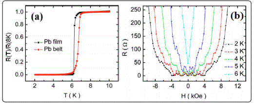
Wang et al [65] produced single-crystal Pb nanobelts of 28 atomic monolayers thick, 285 nm wide, and 10 μm long by focus ion beam technique. In Figure11a, it shows that the onset TC (6.9 K) of the Pb nanobelt is obviously higher than that (6.3K) of the Pb film. Figure 10b shows magnetoresistance oscillations at various temperatures below TC in both positive and negative perpendicular fields. This figure gives evidence that the oscillation in the Pb nanobelt is reproducible (not just some sort of noise) and might be considered quasiperiodic.
It was found for individual thicker Pb nanowires that the material of the electrodes can have a strong influence on the superconducting state, even at distances between the voltage terminals exceeding the superconducting coherence length. Wang et al [65] fabricated single crystal Pb nanowires with two different diameters (55 nm and 70 nm) by electrochemical deposition. R-T, R-H and R-I curves measured by standard fourprobe configuration showed a series of resistance steps with increasing temperature, magnetic field, and excitation current respectively as the superconducting nanowires were approaching the normal state. They attributed these steps to PSCs in the Pb nanowires enhanced by the proximity to the normal Pt electrodes.
Sn nanowires
Bulk tinhas a relatively long coherence length of ξ0≈200 nm. Up to now, studies of superconducting properties of metallic Tinnanowires have revealed very interesting behaviour associated with their reduced physical dimension [66-68]. The onset critical field (Hc) and transition temperature (Tc) can be significantly affected bythe diameter and crystal textures of the nanowires.
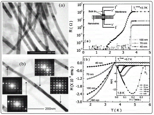
Tian et al. investigated electrical transport properties of the single-crystal tin nanowires with diameters of 40–160nm [66]. The resistance data for all single-crystal wires showed an onset of superconducting transition near 3.7K, the bulk TC of tin. The resistance drop for 40 nm exhibited two distinct regimes below TC, one between 1.7 and 3 K, and another between 3 and 3.7 K, which may be due to a superposition of mally activated phase-slip resistance near TC [67], plus quantum phase-slip (QPS) far below TC [68]. The hc for 40 nm was found to be ~0.3 T at 1.8 K, an order of magnitude higher than that of bulk Sn. These results w ere consistent with the observation of Dubois et al [69] and Michotte et al [52] in Pb wires. However, the M (T) and M (H) curves in single-crystal tin wires did not show their reversibility or hysteretic behaviour observed in the Pb wires Figure 12A. The reversible M(H) curves of tin wires indicates a lack of pinning of residual flux in contract to the interpretation of in Pb wires [70-71].
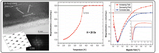
Jankovič et al. fabricated carbon nanotubes encapsulating single crystalline tin nanowires with diameters 15-35 nm by empl oying the catalytic chemical vapour deposition method [72]. The magnetization measurements of Sn-CNT showed a small increase of the Tc (3.72K) onset because of the thinnest nanowires in which the confinement and surface-to-volume ratio becomes large enough to influence the vibrational and electronic properties. The same has been reported in the literature [23] for tin nanowires of 20 nm diameter. Moreover, the Sn-CNT showed a considerable increase (more than 30 times) of the critical magnetic field (Hc0.6 T) compared to bulk metallic tin (0.021 T). The ultrapure tin nanowires are in the clean limit of the microscopic BCS theory, where the mean free path, l, is longer than the coherence length ξ (lξ). In such a case, a nanocylinder of radius R smaller than the coherence length R <ξ and with a magnetic field applied along its axis has a critical field Hc= exp(3/2)Φ0/π2ξR, where Φ0=h/2e is the quantum of flux. Thus, the thinnest wires have a strongly enhanced critical field [73-75].
A noncatalytic and template-free vapour transport process has been employed to prepare s ingle-crystalline Sn nanowires with diameters of 10-20nm [73]. The superconducting transition temperatures for Sn nanowires was about 3.7 K, which was very close to that of bulk β-Sn. Magnetization measurements showed that the critical magnetic fields for both Sn nanowires increased significantly as compared to that of bulk Sn Figure 12B.
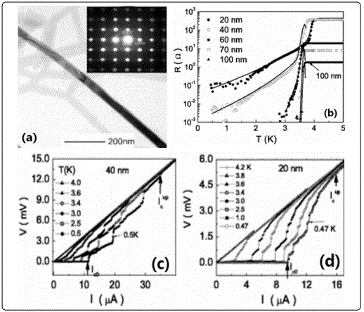
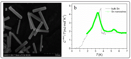
Tian et al. were fabricated Sn nanowires by electrodepositing tin into a porous membrane at room temperature [23]. The wires diameters was 20, 40, 60, 70, and 100nm and the length was about 6μm. The onset temperature Tc of nanowires was found to be close to the bulk value at 3.7K for all wires with d⩾40nm. A slight increase in Tc to 4.1K was found for the thinnest, i.e., 20nm wire. One possible origin was that this was an effect of the increased surface area, wh ich may enhance surface electron-phonon scattering effects [75]. In wires of 40 and 20nm, a clear functional dependence of the residual resistance on temperature was found. The broadening of the transition near Tc in thin whiskers [76-77] and In nanowires has been o bserved and was interpreted as a consequence of a TAPS process [10,78]. The low-temperature exponential residual resistance that extends over a wide range of temperature down to 0.47K could not be understood in the framework of the TAPS model. A similar exponential de cay in resistance down to low temperature was found by Giordano [79] in granular indium wire of 41nm in diameter, fabricated from evaporated In film with step-edge lithographic technique. Giordano proposed a phenomenological QPS model to explain his results. The finite exponentially decaying in resistance is proposed to result from quantum fluctuation-induced tunnelling through an energy barrier ΔF, resulting in a resistance RQPS of the form e-ΔFτGL/ℏ withτGL and ℏ being the Ginzburg-Laudau relaxation time and Planckʼs constant, respectively. The V-I curves of Sn thinner wires demonstrated that the finite resistance measured at the low current limit (I<2μA) was ohmic in nature at all temperatures, which lends further credence to the phenomenological QPS model with a tunnelling energy barrier. The V-I curves for 20 and 40nm wires showed a series of voltage steps in approaching the normal state over the entire temperature range of T<Tc. The V-I characteristics of the Sn wires exhibited features were similar to the experiments of Michotte et al. and consistent with their proposed model. Michotte et al [54] investigated the V-I characteristics of polycrystalline Sn nanowires with 50μm in length and 55nm in diameter fabricated by electrodeposition method. Their results showed two voltage steps in the V-I curve under constant current-driving mode. Michotte et al [52] proposed a model using the generalized time-dependent Ginzburg-Landau equation. The theory indicated that the competition between two relaxation times (relaxation time of the absolute value of the order parameter τ|ψ| and relaxation time of the phase of the parameter τ|ϕ| in the PSC) governs the phase slip process (i.e., τ|ϕ|<τ|ψ). They discussed the effect of magnetic field and defects on both relaxation times and V-I curve. An important conclusion of their model is that under a magnetic field that exceeds a critical value (H*), the voltage jumps (PSCs) disappear in the V-I curve. The reason is that the magnetic field suppresses the order parameter |ψ| everywhere in the sample, leading to an increase of Λq~1/√(|ψ|), and hence there is a lack of space for the coexistence of two PSCs in the wire. The model also predicts that there will be no hysteresis near the voltage steps when the defects in the wire are sufficiently “strong.” However, Figures13c and d showed at least six voltage steps (PSCs) in individual 40nm Sn wire of 6μm in length, and much more PSCs along the length in 20 nm Sn wires than the single 40nm wire. The different results between Tian et al. and Michotte et al. might be single crystalline and polycrystalline morphology.
Zhang et al. synthesized single crystalline Sn nanowires with typical thickness of 60–70 nm in diameter and with average length of 500 n m using surfactant as soft template by a chemical reduction process [80] (Figure 14a). The resistivity data of Sn nanowires showed a strong enhancement of the onset Tc and a high upper critical field(Figure 14b). Herzog et al [1] have reported Tc onsets of much thicker granular Sn nanowires somewhat above 4 K which may have been caused by the granularity. A slight increase in Tc to 4.1K was also found for the 20nm Sn wire po ssible dueto the enhanced surface electron-phonon scattering effects [23]. the large width of the superconducting transition observed in the specific heat was at tributed to a large distribution of different coupling strengths [81,82]. The additional transition in the specific heat at 5.5 K was related to an enhanced effectiv e electron-phonon interaction near the surface of a superconductor [55,83]. In addition, the curvature of the surface may represent another i mportant ingredient for the Tc enhancement in these cylindrical nanowires [84]. Without these effects, the Tc of a superconductor would rather be expected to decrease with dimensionality [85-86]. The critical field of this Sn nanowires (3T) was enhanced by about two orders of magnitude with respect to Sn in its bulk for m (0. 03T), possibly because of the particularly strong spin orbital coupling [87-88] in a metallic surface state band.
Bi nanowires
It is well-known that bulk rhombohedral Bi at ambient pressure is not a superconductor down to 50mk [89]. Recent studies on this “old” material have uncovered a number of new phenomena [68,90]. Rhombohedral Bi nanowires have been observed to become superconducting due to topological nature of the surface state of crystalline Bi in confined geometries [91-93].
Granular Bi nanowires with well-defined rhombohedral grains of ~10 nm diameter, fabricated by electrochemically depositing Bi into porous polycarbonate membranes at ambient pressure [47], were superconducting with two transition temperatures, Tc, of 7.2 and 8.3 K. These Tc values coincide with Tc values of the high-pressure phases Bi-III and Bi-V, respectively. The authors suggested that it could be due to the high-pressure phases existing in the grain boundaries. The sharp voltage steps were also observed in the V-I curves which were very similar to those found in quasi-one-dimensional superconducting nanowires.
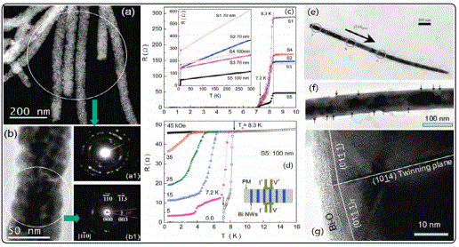
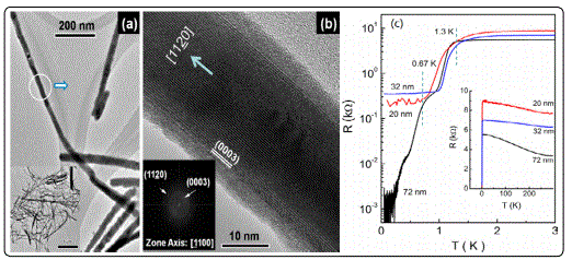
Ye et al [94] reported experimental evidence for superconductivitybelow 0.64K in electrochemically fabricated single-crystal Bi nanowires with a rhombohedral lattice structure of bulk Bi at ambient p ressure. As shown in Figure 15e there were some spots along the nanowire. Tian et al [95] fabricated bamboo-like morphology Bi nanowires with 79 nm in diameter. The high resolution TEM image (Figure 15g) taken near the “bamboo” stripe indicated that the stripes shown in Figure 15f are actually small-angle twinning boundaries with a twinning plane of (1014), which was perpendicular to the growth direction of the wire. The log R-log T plot of (1014) twined Bi nanowires showed a shoulder around 0.67 K which was likely related to the same superconducting phase observed by Ye et al. This would suggest the 0.67 K superconducting phase shown in this paperand results of Ye could have its origin of superconductivity from the twinning planes. The observation of superconductivity below 1.3 K was associated with the interface between the surface oxide and the inner core of the Bi wire.
To further explores the transport properties of individual single-crystalline Bi nanowires, Tian et al. synthesized ultrathin Bi nanowires of 20 and 32 nm diameters(Figure 16a and b). Compared with 72 nm Bi wire,the superconducting transition at 1.3 K was seen in both 20 and 32 nm cylindrical nanowires, but the 0.67 K phase observed in 72 nm wire did not appear (shown in Figure 16c). However, their superconducting critical magnetic fields decreased with their diameter, which is the opposite of the expected behavior for thin superconducting wires. Quasiperiodic oscillations of magneto resistance were observed in perpendicular fields but were not seen in the parallel orientation. This result is also consistent with the observation of superconductivity of Bi confined in an opal host without surface oxidation [96]. The superconductivity in cylindrical nanowires or particles is most likely related to the surface curvature-induced stress in the nanowires or nanoparticles. Such stress will give rise to considerable distortion or disordering in the surface states of the cylindrical nanowires.
Zn nanowires
Bulk zinc (Zn) is a conventional type I superconductor(S) with a transition temperature at 0.85 K and a critical magnetic field of 50 Oe. Its superconducting coherence length in a bulk crystalline sample, ξ0, at T = 0 K is found to be as large as 2.0μm [97], which is almost an order larger than those of the other materials mentioned above. Therefore, one-dimensional (1D) effects in Zn nanowires are expected to be more apparent compared to other wires of the same diameter.
Zinc nanowires with diameters between 40 and 100 nm were fabricated by electro depositing Zn in to commercially available polycarbonate (PC) or anodic aluminium oxide (AAO) membranes. [98], and study was conducted on the transport properties of the Zn nanowires.
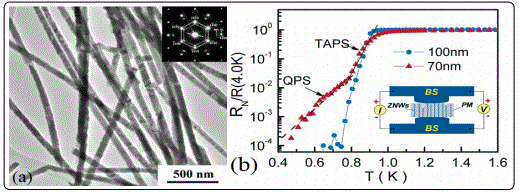
Figure 17b showed the normalized resistance (RN/R (4.0K)) versus temperature (T) of 70- and 100-nm single-crystal Zn nanowires with a length of 6μm, measured at a dc excitation current of 10nA. The onset temperature, Tc, of both nanowires was found to be around 0.93 K, slightly higher than the Tc of bulk Zn (0.84 K). However, the superconducting transition of 100 nm wires was sharp and the resistance drops to zero below 0.75 K (ΔT ≈ 0.17 K). In contrast, the transition of 70 nm wires broadened and showed a residual resistance extending down to 0.55 K. Two distinct linear sections were found. The broadening of the transition near Tc was interpreted as a consequence of a thermally activated phase slip (TAPS) process [134] [135] in a 1D system. The second low-temperature exponential residual resistance that extends over a wide range far below Tcis probably from the quantum phase-slip process suggested first by Giordano. The result with 70-nm Zn wires is also consistent with Tianʼs previous observations of 20- and 40-nm single-crystal Sn nanowires; the only difference is that the resistive tail caused by the QPS process in Zn nanowires appears in relatively larger diameter wires.
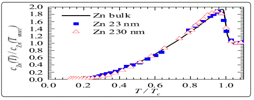
Kurtz et al. probed the thermodynamics of Z n nanowires filling porous anodic alumina membranes (AAMs) with diameters of 230 and 23nm [99]. The critical temperature in zero field, def ined as the midpoint of the jump, for both samples was higher than in bulk (Tcbulk = 0.85K [100]): 0.89 and 0.94 K for the small-pore and large-pore samples, respectively. The enhancement of the transition temperature may be due to local disorder though it is unclear why the larger wires are more affected. The height and breadth of the transition of the samples were plotted in Figure 18. The specific heat jump of bulk Zn crystal was slightly sharper than that of Zn nanowires. The spread in wire diameters in each sample and the dependence of the transition temperature on wire diameter can account for much of this width. The more rounded peak of the large-pore sample would thus be consistent with its larger spread in wire diameter. The height and breadth of the specific heat jump were virtually unaffected by the severe confinement. Evidently, the suppression of superconducting order by thermodynamic fluctuations was much more sensitively detected by electrical transport, since a zero-resistance state depends on long-range phase coherence along the entire length of the sample. Specific heat, on the other hand, probes more local superconducting order, which is apparently still quite robust even in 23 nm diameter nanowires that are nearly 7 times smaller than the coherence length.
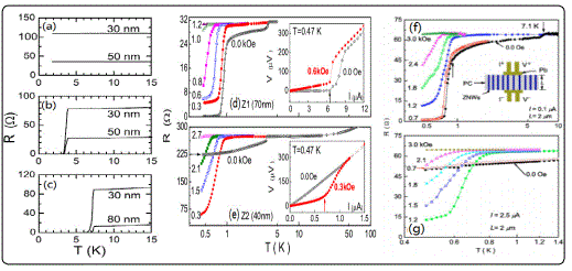
When a superconducting nanowire is connected to two strongly superconducting bulk electrodes, the total combined system is exp ected to be superconducting below the Tc of the superconducting nanowire and the electrodes [101-102]. The superconductivity of the wire is expected to become more robust through its coupling with the superconducting reservoirs. It was observed in Figure 19a-c that single-crystal Zn nanowires of diameter 30–250 nm and length 6μm, using an in situ template-based electrochemical method [103], did not show any signature of superconductivity when they were in contact with Au electrodes, while Zn nanowires were superconducting at Tc(Sn) when they were in contact with Sn electrodes. And were superconducting at Tc(Pb) when they were in contact with Pb electrodes. Liu et al. concluded that when in contact with electrodes having a higher Tc, superconductivity was induced in these NWs at the Tc of the electrodes.
The results of Tian are contrary to this expectation in a system consisting of superconducting zinc nanowires (ZNWs) sandwiched between two bulk superconductors (BSs) of differe nt materials (Sn and In), which showed the strong effect of their superconducting environment [4]. It was found that the superconductivity of Zn nanowires of 40 nm diameter was suppressed either completely or partially by the superconducting electrodes. When the electrodes were driven into their normal state by a magnetic field, the nanowires switched back to their superconducting state. The phenomenon was not seen in wires with diameters equal to or thicker than 70 nm, as shown in Figure 19d and e. However, when Zn nanowires of 40 nm in diameter and two micrometers in length sandwiched between Pb electrodes, the antiproximity effect (APE) found in this system was subtle, showing up primarily in significantly reducing the critical current of the Zn nanowires when the Pb electrodes were in a superconducting state. The critical current was independent of the magnetic field until it was increased to a characteristic value Hd near 0.6 kOe when the critical current showed a rapid enhancement and reaches a maximum value at the critical field of Pb electrodes at 0.94 kOe. The overall features of the R-T curves as shown in Figure 19f and g resembled those found in the 70 nm diameter ZNWs with bulk Sn or In electrodes where the ZNWs and electrodes both show superconductivity at their respective Tc.
Fu et al [104] developed a theory for a superconducting nanowire coupled to various environments. This theory considered the boundary effect and phase-slip interaction in the presence of dissipative environment and suggested that the APE is due to the dissipation at the boundary between the ZNWs and the electrodes. When the nanowire of finite length is placed into a dissipation free environment, the ends of the wire can be mapped onto two parallel boundary lines that can screen the vortex-antivortex interaction of the superconducting order parameter and destroys the superconducting phase even at T=0 K. When the ends of the wire are coupled to a dissipative environment (such as normal metal electrodes), the screening becomes incomplete. As a result, for large dissipation the superconducting phase of the wire is stabilized. However, this model does not address the observation that the “strength” of APE is dependent on the materials of the superconducting electrode materials. Moreover, the APE has been observed only in zinc nanowires.
Al nanowires
A convenient material to study the phenomena associated with QPS mechanismis aluminium. Its bulk critical temperature TCbulk~1.2K is relatively low, hence, the QPS rate should be comparatively high enabling pronounced manifestation ofthe effect. An additional useful feature of aluminium is its peculiar size dependenceof TC. Although the origin of this effect remains unclear, an increase of TC with reduction of the characteristic dimension of aluminium structures (wire diameteror film thickness) is a well-known experimental fact and can be taken as granted [105].
Zgirski et al [5,106-107] showed that the application of low energy (~1keV) Ar+ ion sputtering allows one to progressively and non destructively reduce dimensions of Al nanowireswidth down to 10 nm. The electron mean free pathin such structures was estimated to be about or larger than the specimen thickness and, therefore, such nanowires can be considered to be in the clean limitfor the transverse (confined) electron motion. An evolution of the shape of R(T) dependencies in ul trathin and homogeneous aluminium nanowires as a function of their effective diameter was observed [5]. It was found (as shown in Figure 20) that for effective diameters √σ ≥15 nm the R(T) dependencies can be described by the model of thermally activated phase slips. For thinner wires the width of R(T) transition is dramatically wider, and the resistance may not tend to zero at T→0. They associated this phenomenon with manifestation of quantum phase fluctuations (quantum phase slips). The systematic shift of the mean critical temperature Tc to higher values with reduction of the wire cross section. This is a well-known experimental fact: critical temperature of superconducting films (and wires) often differs from the corresponding bulk value. For aluminium the Tc always increases with the decrease of the minimum characteristic dimension. When the wire diameter was further reduced [106], deviations from the TAPS behaviour became obvious (Figure 20b). Fits to the TAPS model failed to provide any reasonable quantitative agreement with experiment for diameter values belowσ1/2≤20 nm even if one hypothetically assumes the existence of unrealistically narrow constrictions not observed by SPM. The broadening of the R(T) dependencies in aluminium nanowires at T < TCbulk can hardly be ascribed to geometrical imperfections, such as constrictions. On the contrary, the broadened R(T) curves of the thinnest Al samples(Figure 20b) can be nicely fit with the QPS model. One can conclude that the most natural interpretation of the results [34] can be associated with quantum fluctuations.
The observed broad R(T) dependencies in long Al nanowires (up to 100μm)were associated with QPS (Figure 21) [6]. Although rather scarce experimental datamake quantitative conclusions on the QPS mechanism difficult, the experiments on long Al nanowires have a clear message: (a) the width of the experimental R(T) transitions is much larger than predicted by TAPS model, (b) no correlations between the total normal state wire resistance RN (compared to the quantum resistance unit Rq = 6.45 kΩ) and superconductivity in such wires was found. Altomare et al [37] fabricated Al nanowires with 8 nm wide using thermally evaporating aluminium onto a narrow molecular-beam epitaxy (MBE) grown In P ridge. Their results indicated that at higher T(T/Tc ≥0.7) the contribution from QTPS is negligible compared to TAPS, at low T (T/Tc≤ 0.5) TAPS is expected to be exponentially suppressed and QTPS should dominate. This expectation was confirmed by the fits which yielded a negligible RTAPS compared to RQTPS, as shown in Figure 22.
Solid colorlines stand for fits using TAPS (blue) and QPS (red) contributions
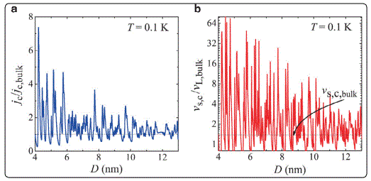
Croitoru et al [108] investigated the influence of the quantum size resonances on the critical magnetic field and the critical supercurrent in Al cylinder nanowire with diameter D =3-15 nm and length L =5μm λF based on a self-consistent numerical solution of the Bogoliubov–de Gennes equations. The formation of single-electron sub bands as a consequence of quantum confinement strongly influenced the superconducting-to-normal phase transition driven by a magnetic field. According to the Ginzburg–Landau theory this transition is of second order for mesoscopic wires, while being of first order in bulk type I superconductors. However, the situation changes significantly for narrower wires. As shown in Figure 23, in a parallel magnetic field and/or in the presence of a supercurrent the transition from the superconducting to the normal phase occurred as a cascade of discontinuous jumps in the superconducting order parameter for diameters D < 10~15 nm at T = 0. The critical magnetic field exhibited quantum-size oscillations with pronounced resonant enhancements as a function of the wire radius.
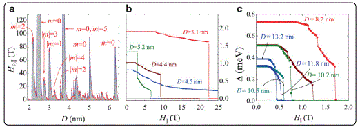
Figure 24a showed the calculated critical current density as a function of the nanowire diameter. This result showed that quantum-size effects play a very important role in the size-dependent increase of the critical current. Real samples exhibit inevitable cross-section fluctuations that will smooth those quantum-size oscillations in the critical current. Figure 24b displayed the critical superfluid velocity vscas a function of the wire diameter. This quantity defined as the velocity at which complete destruction of the condensate occurs exhibits the same trend.
W nanowires
Focused ion beams (FIB) technique offers the means to rapidly develop nanoscale devices in a single processing step in situ without the demand of time-consuming mask fabrication or extensive prior sample preparation. Tungsten is one of the most commonly used materials in FIB.
Córdoba [109] dealed with the growth of superconducting W NWs and W ultranarrow NWs grown by FIBID, with lateral size of by FIBID with lateral size ~200 nm and ~50 nm respectively. The magnetic field dependence R(B) of the resistance of the W ultranarrow NWs showed non-monotonic R(B) behaviour and re-entrant zero-resistance state at lower temperature. At B<BV=1.61 s (φ0/w2), the dissipation was caused by the ‘external’ vortices crossing the wire. Every vortex saw a dome-like potential barrier with the maximum at the strip center and the height linearly decreasing with B.At B = BV, a single row of equilibrium vortices settled in the middle of the wire. Thus, at B>BV the dissipation was governed by the escape of these vortices from the strip across the barriers created by edge superconductivity. At B≈BV, the newly established edge barriers were nearly zero. As they also vanish at B = Bc3 = 1.695Bc2, where Bc2 = φ0/2πξd2 (T), where superconductivity was fully suppressed, these barriers must achieved their maximal value at some field between BV and Bc3, giving rise to the N-shape of R(B) with the maximum at BV.In addition to the re-entrance of the dissipation-free state observed in superconducting ultranarrow NWs a, the fundamental differences detected from structures of different lateral width were Jc and Bc2,2K. The critical current density without external magnetic field in superconducting W ultranarrow NWs was one order of magnitude higher than the values obtained in both microwires and nanowires. In a bulk material, as W nanowires and microwires may be considered, the critical current density is governed by the pinningforces. However, if the dimensions of the structures are reduced to values close to ξ, superconductivity is preserved at the edges of the structures, so high current density is needed to be applied to overcome the energy barrier [110-112]. However, the upper critical field in the superconducting W ultranarrow NWs was at least a factor of 1.5 lower than the results obtained in W nanowires and microwires.This behaviour would be given by the energy dissipation mechanism, which holds exclusively in this kind of ultranarrow nanostructures in which width or thickness are of the same order as the coherence length.
Using the technique of FIB-CVD, Li et al [113] have grown ultra-thin and ultra-narrow tungsten lateral nanowires with width and thickness comparable to the phase coherence length (ξ) of the bulk material. Temperature-dependent electrical measurements showed that the wires were conducting and had a superconducting transition with a transition temperature (Tc) about 5.1 K. Resistance vs. temperature measurements revealed that (Figure 26) with decreasing cross-sectional area, the wires display an increasingly broad superconducting transition. A residual resistive tail extending down to the low-temperature region was found only for the thinnest tungsten nanowire, which is 10nm thick and 19nm wide. The logarithm of the residual resistance of this wire appeared as two linear sections as a function of temperature, one within 300mK below Tc and the other extending down to the lowest measuring temperature of 4.26 K. Such features have previously been identified with phase slip processes as discussed before.
Conclusion
Remarkable progresses in quasi-one-dimensional superconducting single crystal nanostructures fabrication have been made in the past few years. Various techniques were employed, including directional deposition onto step edges, sputter deposition onto suspended carbon nanotube (CNT), electro deposition into porous membranes, etch thinning of thick wires, superlattice nanowire pattern transfer (SNAP) method, chemical vapour deposition method, and solution-phase method. The superconducting single crystal nanowires are suitable for the establishment of the quantitative agreement between the theory and experiment. The key conclusions of these investigations can be summarized as follows. Fluctuations play an important role in high-quality metallic superconductors with nanoscale dimensions. In relatively thick samples, the finite width of experimental R(T) transition can be qualitatively understood within the formalism of thermally activated phase slips (TAPS). Upon reduction of the wire diameter, the QPS rate increases drastically. If the wire diameter is decreased further (diameters ≤ 10 nm), QPS proliferate causing a sharp crossover from a superconducting to a normal behaviour. The critical magnetic field exhibits quantum-size oscillations with pronounced resonant enhancements in thinner nanowires. However, the origin of the TC size dependence phenomenon is not clear yet. The thinner single crystalline niobium and aluminium nanowires have a lower Tc; the thinner single crystalline tin nanowires have higher TC, may be because of surface electron-phonon scattering effects; single crystal lead wires show higher Tc than that of polycrystalline ones, but no size dependence is observed.
Acknowledgements
This work was financially supported by the National Natural Science Foundation of China (No. 51271215) and the Innovative Exploratory Grant of Hong Kong University of Science and Technology (No. IEG14EG02PG).
References
- Herzog AV, Xiong P, Sharifi F, Dynes RC. Observation of a Discontinuous Transition from Strong to Weak Localization in 1D Granular Metal Wires. Phys. Rev. Lett. 1996; 76: 668. doi: 10.1103/PhysRevLett.76.668
- Camarota B, Parage F, Delsing P, Buisson O. Experimental Evidence of One-Dimensional Plasma Modes in Superconducting Thin Wires. Phys. Rev. Lett. 2001; 86: 480. doi: 10.1103/PhysRevLett.86.480
- Fabio A, Chang AM, Michael RM, Yuguang H, Charles WT. Evidence for Macroscopic Quantum Tunneling of Phase Slips in Long One-Dimensional Superconducting Al Wires. Physical Review Letters. 2006; (97): 017001. doi: 10.1103/PhysRevLett.97.017001.
- Boogaard GR, Verbruggen AH, Belzig W, Klapwijk TM. Resistance of superconducting nanowires connected to normal-metal leads. Phys. Rev. B. 2004; 69: 220503. doi: 10.1103/PhysRevB.69.220503
- Blonder GE, Tinkham M, Klapwijk TM. Transition from metallic to tunnelling regimes in superconducting micro constrictions: Excess current, charge imbalance, and supercurrent conversion. Phys. Rev. B. 1982; 25: 4515. doi: 10.1103/PhysRevB.25.4515
- Maki K, Fulde P. Equivalence of Different Pair-Breaking Mechanisms in Superconductors. Phys. Rev. 1965; 140: A1586. doi: 10.1103/PhysRev.140.A1586
- Yi G, Schwarzacher W. Single crystal superconductor nanowires by electrodeposition. Appl. Phys. Lett. 1999; 74(12): 1746-1748. doi: 10.1063/1.123675
- Lin YH, Nelson J, Goldman AM. Superconductivity of very thin films: the superconductor-insulator transition. Phys. C. 2015; 514:130-141. doi: 10.1016/j.physc.2015.01.005
- Kim H, Jamali S, Rogachev A. Superconductor-insulator transition in long MoGe nanowires. Phys. Rev. Lett. 2012; 109(2): 0270021-0270025. doi: 10.1103/PhysRevLett.109.027002
- Dickey JM, Paskin A. Phonon spectrum in small particles and their implications for superconductivity. Phys. Rev. Lett. 1968; 21(20): 441-1443. doi: 10.1103/PhysRevLett.21.1441
- McMillan WL. Transition temperature of strong-coupled superconductors. Phys. Rev. 1968; 167 (2): 331–344. doi: 10.1103/PhysRev.167.331
- Eugene BG, Alexey VB, Alexander VK, Vladimir IM, Igor IK. Suppression of superconductivity in thin Nb nanowires fabricated in the vortex cores of superfluid helium. Physica C. 2015; 516: 44–49. doi: 10.1016/j.physc.2015.06.010
- Tinkham M, Lau CN, Markovic N. Resistance induced by quantum phaseslips in superconducting nanowires. Physica E. 2003; 18(1-3): 308-311. doi: 10.1016/S1386-9477(02)01033-0
- Wang J, Shi CT, Tian ML, et al. Proximity-induced superconductivity in nanowires: minigap state and differential magneto resistance oscillations. Phys. Rev. Lett. 2009; 102(24): 247003-247006. doi: 10.1103/PhysRevLett.102.247003
- Wang J, Ma XC, Lu L, et al. Anomalous magneto resistance oscillations and enhanced superconductivity in single-crystal Pb nanobelts. Appl. Phys. Lett. 2008; 92(23): 233119. doi: 10.1063/1.2945280
- Wang J, Ma XC, Qi Y, et al. Carrier transport properties of nanocrystalline Er3N@C80. J. Appl. Phys. 2009; 106: 034301. doi: 10.1063/1.4887796
- Wang J, Jia JF, Ma XC, et al. Semiconductor-superconductor transition and magneto resistance terraces in an ultrathin superconducting Pb nanobridge. J. Vac. Sci. Technol. B. 2010; 28: 678. doi: 10.1116/1.3437016
- Guan ZL, Ning YX, Song CL, et al. Sample-size dependence of the superconducting transition of ribbon-shaped Pb nanocrystals studied by scanning tunneling spectroscopy. Phys. Rev. B. 2010; 81: 054516. doi: 10.1103/PhysRevB.81.054516
- Michotte S, Piraux L, Dubois S, Pailloux F, Stenuit G, Govaerts J. Superconducting properties of lead nanowires arrays. Physica C. 2002; 377(3): 267–276. doi: 10.1016/S0921-4534(01)01306-5
- Michotte S, Mátéfi TS, Piraux L. 1D-transport properties of single superconducting lead nanowires. Physica C. 2003; 391(4): 369–375. doi: 10.1016/S0921-4534(03)01086-4
- Kramer L, Watts RJT. Theory of Dissipative Current-Carrying States in Superconducting Filaments. Phys. Rev. Lett. 1978; 40: 1041. doi: 10.1103/PhysRevLett.40.1041
- Ohshima K, Fujita T. Enhanced Superconductivity in Layers of Ga Fine Particles. J. Phys. Soc. Jpn. 1986; 55: 2798–2802. doi: 10.1143/JPSJ.55.2798
- Cohen RW, Abeles B. Superconductivity in Granular Aluminum Films. Phys. Rev. 1968; 168: 444–450. doi: 10.1103/PhysRev.168.444
- Fulde P, Ferrell RA. Superconductivity in a Strong Spin- Exchange Field. Phys. Rev. 1964; 135: A550–A563. doi: 10.1103/PhysRev.135.A550
- Wang J, Ma X, Lu L, et al. Anomalous magneto resistance oscillations and enhanced superconductivity in single-crystal Pb nanobelts. Appl. Phys. Lett. 2008; (92): 233119. doi: 10.1063/1.2945280
- Dubois S, Michel A, Eymery JP, Duvail JL, Piraux L, Mater J. Fabrication and properties of arrays of superconducting nanowires. Res. 1999; (14): 665-671. doi: 10.1557/JMR.1999.0091
- McCumber DE, Halperin BI. Time Scale of Intrinsic Resistive Fluctuations in Thin Superconducting Wires. Phys. Rev. B. 1970; (1): 1054. doi: 10.1103/PhysRevB.1.1054
- Han JE, Crespi VH. Asymmetry in negative differential resistance driven by electron-electron interactions in two-site molecular devices. Phys. Rev. B. 2004; (69): 214526. doi: 10.1063/1.1413499
- Naugle DG, Baker JW, Allen RE. Evidence for a Surface-Phonon Contribution to Thin-Film Superconductivity: Depression of Tc by Noble-Gas Overlayers. Phys. Rev. B. 1973; (7): 3028. doi: 10.1103/PhysRevB.7.3028
- Lukens JE, Warburton RJ, Webb WW. Onset of Quantized Thermal Fluctuations in “One-Dimensional” Superconductors . Phys. Rev. Lett. 1970; 25: 1180. doi: 10.1103/PhysRevLett.25.1180
- Newbower RS, Beasley MR, Tinkham M. Fluctuation Effects on the Superconducting Transition of Tin Whisker Crystals. Phys. Rev. B. 1972; 5: 864. doi: 10.1103/PhysRevB.5.864
- Langer JS, Ambegaokar V. Intrinsic Resistive Transition in Narrow Superconducting Channels. Phys. Rev. 1967; 164: 498. doi: 10.1103/PhysRev.164.498
- Giordano N. Dissipation in a one-dimensional superconductor: evidence for macroscopic quantum tunneling. Phys. Rev. Lett. 1990; 41: 6350. doi: 10.1103/PhysRevB.41.6350
- Pracht US, Bachar N, Benfatto L, et al. Enhanced Cooper pairing versus suppressed phase coherence shaping the superconducting dome in coupled aluminum nanograins. Phys Rev. B. 2016; 93: 100503(R). doi: 10.1103/PhysRevB.93.100503
- Hohenberg PC. Existence of long range order in one and two dimensions. Phys. Rev. 1967; 158: 383–386. doi: 10.1103/PhysRev.158.383
- Mermin ND, Wagner H. Absence of ferromagnetism or antiferromagnetism in one- or two-dimensional isotropic Heisenberg models. Phys. Rev. Lett. 1966; 17: 1133–1136. doi: 10.1103/PhysRevLett.17.1133
- Overcash DR, Ratnam BA, Skove MJ, Stillwell EP. Persistent metallic behaviour of thin bismuth whiskers. Phys. Rev. Lett. 19; 44: 1348. doi: 10.1103/PhysRevLett.44.1348
- Nikolaeva A, Gitsu D, Konopko L, Graf MJ, Huber TE. Quantum interference of surface states in bismuth nanowires probed by the Aharonov-Bohm oscillatory behaviour of the magnetoresistance. Phys. Rev. B. 2008; 77: 075332.
- Zuxin Y, Hong Z, Haidong L, Wenhao W, Zhiping L. Evidence for superconductivity in single crystalline Bi nanowires. Physica B. 2008; 403: 1529–1530. doi: 10.1016/j.physb.2007.10.180
- Seidel G, Keesom PH. Specific Heat of Gallium and Zinc in the Normal and Superconducting States. Phys. Rev. 1958; 112: 1083.
- Cetas TC, Holste JC, Swenson CA. Heat Capacities from 1 to 30 K of Zn, Cd, Sn, Bi, and Y. Phys. Rev. 1969; 182: 679.
- Agassi D, Cullen JR. Current-phase relation in an intermediately coupled superconductor-superconductor junction. Phys Rev. B. 1996; 54: 10112.”
- Haidong L, Zuxin Y, Zhiping L, Rathnayaka KDD, Wenhao W. Boundary effect on superconductivity in long single-crystal superconducting nanowires. Physica C. 2008; 468: 304–309. doi: 10.1016/j.physc.2007.08.029
- Tahara S, Anlage SM, Halbritter J, Eom CB, Fork DK, Geballe TH, Beasley MR. Critical currents, pinning, and edge barriers in narrow YBa2Cu3O7–d thin films. Phys. Rev. B. 1990; 41(16): 11203–11208.
- Jones WA, Barnes PN, Mullins MJ, et al. Impact of edge-barrier pinning in superconducting thin films. Appl. Phys. Lett. 2010; 97(26): 262503. doi: 10.1063/1.3529945
- Elistratov AA, Vodolazov DY, Maksimov IL, Clem JR. Field-dependent critical current in type-II superconducting strips: combined effect of bulk pinning and geometrical edge barrier. Phys. Rev. B. 2002; 66(22): 220506.
