


International Conference on Materials Science and Research
November 16-18, 2017 Dubai, UAE
Conjugated Polymerʼs Side Chains Post-Processing for Improved Molecular Packing and Mobility of Organic Thin-Film Transistors (OTFTs)
1Department of Chemistry, Texas A&M University at Qatar, Qatar
2University of Michigan, Materials Science and Engineering, USA
Soluble conjugated polymers have nowadays attracted broad academic and industrial spotlight as innovative materials of easy tuneable optical and electronic properties.1 These properties translate into various optoelectronic applications such as organic solar cells, light-emitting diodes (LEDs), and thin film transistors. The pivotal parameters that define characteristics of conjugated polymer based devices are of chemical (structure, solubility, mass) and mechanical (macroscopic) nature.2 Although the physical properties CPs is determined by designed chemical structure, critical alterations result from variations of the nanostructure of the polymer in its solid state.3 Therefore the complete optoelectronic potential of CP based device can be fully assessed only with the optimal conjugated chains alignment.
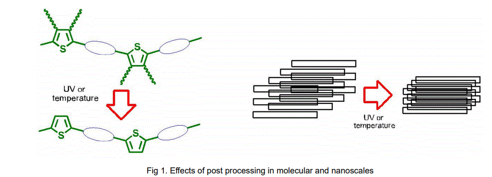
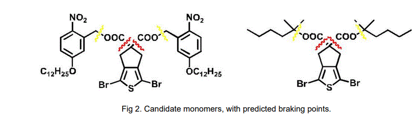
We envisioned thermal and UV induced post processing of conjugated polymers predesigned to dramatically change their properties in given conditions by removal of nonconductive side chains and reducing interlayer distance.
1. A. J. Heeger, Chem. Soc. Rev. 2010, 39 2354∇2371.
2. Kline, R. J., McGehee M. D. Journal of Macromolecular Science Part C: Polymer Reviews, 46: 27∇45,
3. Chung, K. MRS Communications, 2015, 5(2), pp. 169∇189.
